RAYPCB manufactures and assembles high-density interconnect PCBs with blind, buried, and micro-vias, built-up laminations, and the highest signal integrity in the industry.
I’ve been designing HDI PCBs for over a decade now, and I still remember the first time I had to route a 0.4mm pitch BGA on a conventional board. It was a nightmare. The traces were too wide, the vias took up too much space, and I ended up needing 12 layers just to break out from one chip. That’s when I really understood why HDI PCB technology exists—and why every serious PCB engineer needs to master it.
In this guide, I’ll walk you through everything you need to know about HDI PCB technology in 2026. Whether you’re trying to understand the basics or looking to optimize your next high-density design, this article covers the fundamentals, the different types, design guidelines, stackup configurations, and the manufacturing process. Let’s dive in.
An HDI PCB (High-Density Interconnect Printed Circuit Board) is a type of circuit board that packs more wiring density per unit area than conventional PCBs. According to IPC-2226, the international standard for HDI design, these boards are characterized by:
What makes HDI PCB technology special is its use of microvias—laser-drilled holes typically ranging from 50 to 150 microns in diameter. These tiny vias, combined with blind and buried via structures, allow designers to create compact, high-performance boards that would be impossible with traditional through-hole technology.
The push toward smaller devices with more functionality has made HDI PCB technology essential. Your smartphone, for instance, contains a motherboard that would have filled an entire desktop computer just 20 years ago. This miniaturization is possible because HDI PCB technology allows:
The global HDI PCB market was valued at approximately $16.2 billion in 2024 and is projected to reach $24.8 billion by 2029, according to industry research. This growth reflects just how fundamental HDI technology has become across consumer electronics, automotive, medical devices, and telecommunications.

Understanding the distinction between HDI PCB and conventional PCB is crucial for making the right design decisions. I’ve worked on projects where clients initially pushed for HDI when conventional boards would have sufficed, and others where they tried to force a design onto standard technology when HDI was clearly needed. Knowing when to use each saves both time and money.
The fundamental difference comes down to interconnect density. A standard PCB relies on mechanically drilled through-holes that span the entire board thickness. These through-holes have practical minimum diameters around 200-250 microns due to drill bit limitations. HDI PCB, in contrast, uses laser-drilled microvias that can be as small as 50 microns and only connect adjacent layers.
Here’s a detailed comparison:
| Feature | Standard PCB | HDI PCB |
|---|---|---|
| Minimum Trace Width | 100-150 µm (4-6 mils) | 50-75 µm (2-3 mils) |
| Minimum Via Diameter | 250-300 µm (10-12 mils) | 50-150 µm (2-6 mils) |
| Via Type | Through-hole vias only | Microvias, blind, buried, stacked |
| Drilling Method | Mechanical drilling | Laser drilling + mechanical |
| Layer Count for Same Function | Higher (8-12 layers) | Lower (4-6 layers) |
| Aspect Ratio | Up to 8:1 | 0.75:1 to 1:1 for microvias |
| BGA Pitch Supported | ≥0.8mm | Down to 0.25mm |
| Manufacturing Cost | Lower | Higher (1.5x to 4x) |
| Lead Time | Shorter | Longer (sequential lamination) |
The key takeaway? HDI PCB isn’t just about making things smaller—it’s about enabling designs that simply cannot exist with conventional technology. When you’re working with modern fine-pitch BGAs, high-speed DDR memory interfaces, or compact IoT devices, HDI becomes a necessity rather than a luxury.
RAYPCB Engineering Tools
HDI (High Density Interconnect) PCBs use microvias, blind/buried vias, and fine lines to achieve higher routing density. Select the appropriate type based on your design complexity and component requirements.
One buildup layer on each side of the core. Single laser drilling step. Most cost-effective HDI option.
Two buildup layers each side with stacked or staggered microvias. Higher density for complex BGAs.
Three buildup layers with stacked microvias and buried vias in the core. Premium density solution.
Every layer interconnected through stacked copper-filled microvias. Maximum routing flexibility.
| Design Rule | Your Value | Min Required | Max Allowed | Status |
|---|---|---|---|---|
| Line Width | 75 μm | 50 μm | — | ✓ Pass |
| Line Spacing | 75 μm | 50 μm | — | ✓ Pass |
| Microvia Diameter | 100 μm | 75 μm | 150 μm | ✓ Pass |
| Microvia Aspect Ratio | 0.75:1 | — | 1:1 | ✓ Pass |
| Annular Ring | 75 μm | 50 μm | — | ✓ Pass |
| Pad-to-Pad Clearance | 100 μm | 75 μm | — | ✓ Pass |
| Via-to-Via Pitch | 350 μm | 250 μm | — | ✓ Pass |
| Solder Mask Registration | 50 μm | — | 75 μm | ✓ Pass |
Estimates are approximate. Contact your PCB manufacturer for accurate quotes.
This reference guide provides typical industry specifications. Always verify requirements with your specific PCB manufacturer as capabilities may vary.
HDI PCB structures are classified based on their buildup configuration and via arrangements. The IPC-2226 standard defines six types (Type I through Type VI), but in practice, most designs fall into three main categories plus the advanced Any-Layer HDI option.
Type I HDI represents the simplest and most cost-effective entry into high-density interconnect technology. The notation “1+N+1” means:
In this configuration, you have a single layer of microvias connecting the outer layer to the first inner layer on each side. The core layers use conventional through-hole vias for interconnection.
Specifications for 1+N+1 HDI PCB:
| Parameter | Typical Value |
|---|---|
| Minimum BGA Pitch | 0.4mm |
| Microvia Diameter | 75-100 µm |
| Microvia Depth | 60-80 µm |
| Buildup Layer Thickness | 60-100 µm |
| Cost Multiplier vs Standard | 1.3x – 1.5x |
Best Applications: Basic smartphones, GPS devices, memory cards, tablets, and other consumer electronics that need moderate density improvements.
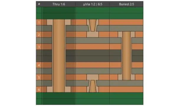
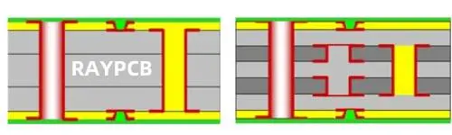
Type II HDI steps up the complexity with two buildup layers on each side of the core. This structure supports either stacked or staggered microvia configurations:
Key Characteristics of 2+N+2 HDI PCB:
| Parameter | Typical Value |
|---|---|
| Minimum BGA Pitch | 0.35mm |
| Sequential Lamination Cycles | 2 |
| Microvia Configuration | Stacked or staggered |
| Cost Multiplier vs Standard | 1.8x – 2.5x |
The 2+N+2 configuration is probably the most popular HDI stackup for complex designs. It strikes a good balance between routing density, manufacturing complexity, and cost.
Best Applications: High-end smartphones, advanced gaming consoles, automotive ECUs, and network equipment.

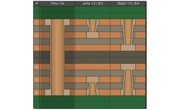
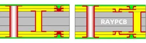
When 2+N+2 isn’t enough, Type III HDI with 3+N+3 or even 4+N+4 structures come into play. These configurations offer:
However, with each additional buildup layer, manufacturing complexity and cost increase substantially. Many fabricators recommend staying at 2+N+2 or 3+N+3 unless absolutely necessary.
| HDI Type | Lamination Cycles | Cost Multiplier | Typical Applications |
|---|---|---|---|
| 1+N+1 | 1 | 1.3-1.5x | Consumer electronics |
| 2+N+2 | 2 | 1.8-2.5x | High-end mobile, automotive |
| 3+N+3 | 3 | 2.5-3.5x | 5G infrastructure, AI processors |
| 4+N+4 | 4 | 4x+ | Cutting-edge computing, aerospace |
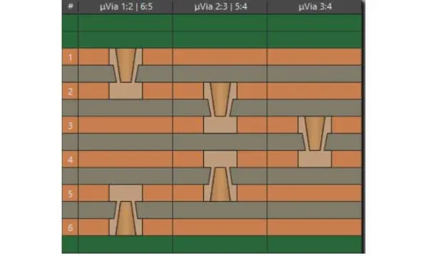
Every Layer Interconnect (ELIC), also called Any-Layer HDI, represents the pinnacle of HDI technology. In ELIC designs:
ELIC is commonly used in flagship smartphones (like those from Apple and Samsung), advanced CPUs/GPUs, and cutting-edge AI accelerators. The cost premium is significant (4-6x vs standard PCB), but for applications where space is at an absolute premium, there’s no substitute.
Designing an HDI PCB requires careful attention to details that might seem minor but can make or break manufacturability and performance. Here are the critical guidelines I follow in my own designs.
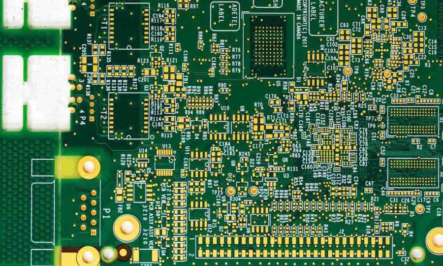
Microvias are the heart of HDI PCB technology, and getting their design right is essential. In my experience, via-related issues account for a significant portion of HDI manufacturing problems. Understanding these rules thoroughly will save you countless revision cycles.
The aspect ratio—the ratio of via depth to diameter—is perhaps the most critical parameter. A microvia with a 100-micron diameter and 100-micron depth has a 1:1 aspect ratio. Why does this matter? When the aspect ratio exceeds 1:1, the copper plating solution cannot adequately reach the bottom of the via during electroplating. This leads to voiding (air pockets in the copper fill) which can cause failures during thermal cycling.
Microvia Specifications:
| Parameter | Recommended Value | Notes |
|---|---|---|
| Diameter | 75-150 µm | Smaller requires UV laser |
| Aspect Ratio | ≤0.75:1 to 1:1 | Critical for reliable plating |
| Capture Pad | 250-350 µm | Larger than via by 100µm+ |
| Target Pad | 200-300 µm | On landing layer |
| Annular Ring | ≥50 µm | Minimum for manufacturing |
Stacking Rules:
HDI PCB designs push traces to their limits:
| Design Class | Trace Width | Spacing | Application |
|---|---|---|---|
| Standard HDI | 75/75 µm | 75 µm | Most HDI designs |
| Advanced HDI | 50/50 µm | 50 µm | High-density BGA fanout |
| Ultra HDI | 30/30 µm | 30 µm | Cutting-edge designs |
Important Considerations:
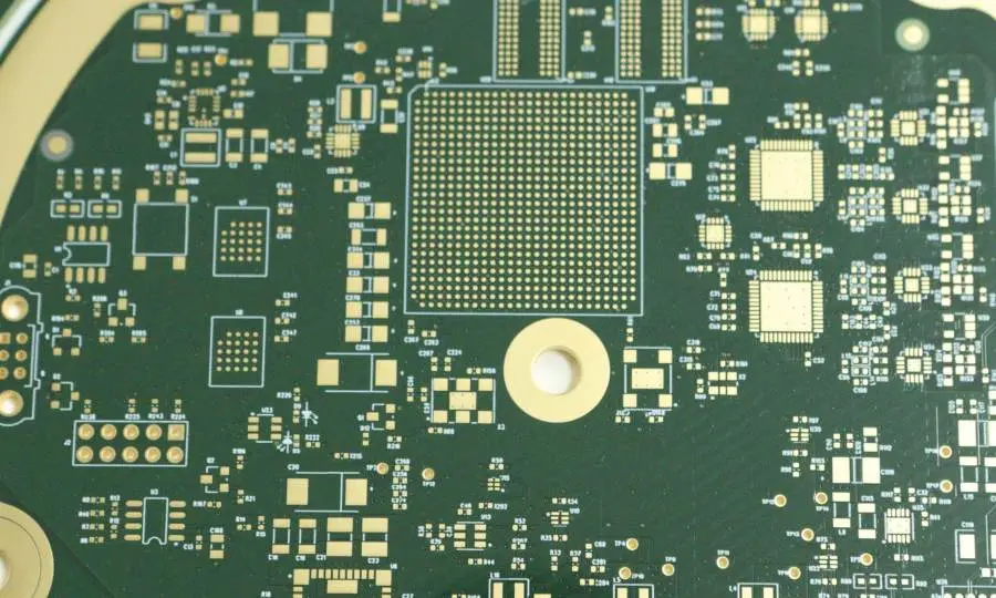
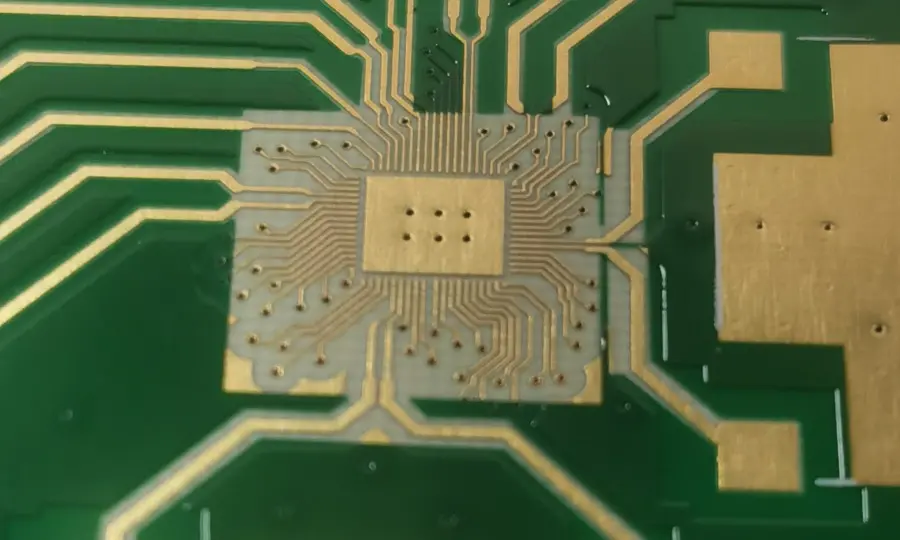
One of the main reasons for using HDI PCB technology is BGA fanout. Here’s how different via strategies enable various BGA pitches:
| BGA Pitch | Via Type | Fanout Strategy |
|---|---|---|
| ≥1.0mm | Standard through-hole | Dog bone with PTH |
| 0.8mm | Microvia | Dog bone with microvia |
| 0.65mm | Via-in-pad | Microvia directly in pad |
| 0.5mm | Via-in-pad + HDI | Filled microvia in pad |
| 0.4mm | 1+N+1 or 2+N+2 | Stacked/staggered microvias |
| ≤0.35mm | 2+N+2 or ELIC | Multiple stacked microvias |
HDI boards often carry high-speed signals, making signal integrity a major concern:
Dense HDI PCB designs concentrate heat in smaller areas:

The stackup is the foundation of any HDI PCB design. Getting it right affects everything from signal integrity to manufacturing yield.
The i+N+i notation describes the HDI buildup structure:
For example, a 2+4+2 stackup has:
Here are typical stackup configurations I use for different applications:
6-Layer 1+4+1 HDI Stackup:
| Layer | Type | Thickness | Purpose |
|---|---|---|---|
| L1 | Signal | 35µm Cu | Top routing + components |
| Prepreg | Dielectric | 75µm | Microvia dielectric |
| L2 | Ground | 35µm Cu | Reference plane |
| Core | Dielectric | 400µm | Core dielectric |
| L3 | Power | 35µm Cu | Power distribution |
| Prepreg | Dielectric | 100µm | Lamination |
| L4 | Ground | 35µm Cu | Reference plane |
| Core | Dielectric | 400µm | Core dielectric |
| L5 | Signal | 35µm Cu | Inner routing |
| Prepreg | Dielectric | 75µm | Microvia dielectric |
| L6 | Signal | 35µm Cu | Bottom routing + components |
Total Thickness: ~1.2mm
Material choice significantly impacts HDI PCB performance:
| Material Type | Dk Value | Df Value | Tg | Best For |
|---|---|---|---|---|
| Standard FR-4 | 4.2-4.5 | 0.02 | 130-140°C | General HDI |
| High-Tg FR-4 | 4.2-4.5 | 0.02 | 170-180°C | High reliability |
| Mid-Loss (Megtron 4) | 3.8-4.0 | 0.005-0.008 | 175°C | High-speed digital |
| Low-Loss (Megtron 6) | 3.4-3.6 | 0.002-0.004 | 185°C | RF, mmWave |
| Rogers RO4350B | 3.48 | 0.004 | 280°C | RF applications |
Material Selection Tips:
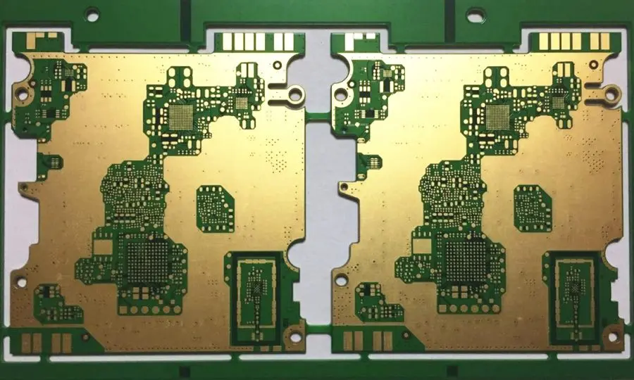
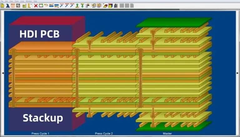
Understanding the manufacturing process helps you design more manufacturable boards. HDI PCB manufacturing differs significantly from conventional PCB fabrication, and this knowledge has saved me from countless design mistakes over the years.
The complexity of HDI manufacturing explains both its higher cost and longer lead times. While a conventional 4-layer board might go through the press once and be done, an HDI board with a 2+N+2 structure goes through the press four times, with drilling, plating, and imaging steps between each lamination cycle.
Unlike conventional PCBs that are laminated in a single step, HDI PCBs use sequential lamination:
For a 2+N+2 stackup, this means at least 4 lamination cycles (one for the core, plus one for each buildup layer on each side).
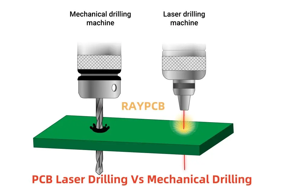
Laser drilling is what makes microvias possible:
Laser Types for HDI PCB:
| Laser Type | Wavelength | Hole Size | Best For |
|---|---|---|---|
| CO2 | 10.6 µm (IR) | 75-150 µm | RCC, non-glass materials |
| UV (Nd:YAG) | 355 nm | 25-100 µm | Glass-reinforced materials |
| UV Excimer | 248/308 nm | <50 µm | Ultra-fine microvias |
| CO2 + UV Combo | Both | 50-150 µm | Production flexibility |
Key Laser Drilling Parameters:
After laser drilling, microvias need to be metallized:
For stacked microvias, copper filling is essential to provide a solid base for the next via.
HDI PCBs require more rigorous testing than conventional boards:
| Test Type | Purpose | Standard |
|---|---|---|
| Microsection Analysis | Via quality, layer thickness | IPC-A-600 |
| Impedance Testing | Verify controlled impedance | IPC-2141 |
| Flying Probe | Electrical continuity | IPC-9252 |
| X-Ray Inspection | Layer alignment, via fill | Internal |
| Thermal Cycling | Reliability verification | IPC-TM-650 |
HDI PCB technology has become essential across multiple industries. Understanding where and why HDI is used helps designers appreciate the requirements and constraints specific to each application.
This sector drives the majority of HDI PCB demand and has been the primary force pushing HDI technology forward:
Modern vehicles are essentially computers on wheels, and the automotive sector has become one of the fastest-growing markets for HDI PCB:
Automotive HDI must meet IATF 16949 quality standards and often requires extended temperature range operation (-40°C to +125°C). The reliability requirements are significantly higher than consumer electronics, with expected lifetimes of 15+ years.
Healthcare relies heavily on compact, reliable electronics, and HDI enables life-saving miniaturization:
Medical HDI PCBs require ISO 13485 certification and extreme reliability. Failure is simply not an option when patient lives are at stake.
The 5G rollout has accelerated HDI adoption significantly:
Mission-critical applications demand the highest reliability and often the most advanced HDI technology:
HDI PCBs cost more than conventional boards, but smart design choices can control expenses. Understanding where costs come from allows you to make informed trade-offs between performance and budget.
The cost premium for HDI comes from several factors. First, the equipment: laser drilling machines cost millions of dollars and require specialized maintenance. Second, the process: sequential lamination means the board goes through the fabrication cycle multiple times, with each cycle adding time and opportunities for defects. Third, yields: tighter tolerances mean more boards fail inspection.
However, I’ve seen many cases where HDI actually reduced total product cost. How? By enabling smaller boards (less material), fewer layers (less processing), and smaller enclosures (less mechanical cost). The key is to optimize the HDI design itself.
| Factor | Impact | How to Optimize |
|---|---|---|
| Layer Count | High | Maximize routing efficiency per layer |
| HDI Structure | High | Use 1+N+1 if 2+N+2 isn’t necessary |
| Via Stacking | Medium | Staggered vias cost less than stacked |
| Trace/Space | Medium | Stay at 75/75 µm if possible |
| Materials | High | Use standard FR-4 unless specs require otherwise |
| Panel Size | Medium | Design for optimal panel utilization |
| HDI Type | Relative Cost | Lead Time |
|---|---|---|
| Standard PCB | 1x | 5-7 days |
| 1+N+1 HDI | 1.3-1.5x | 10-14 days |
| 2+N+2 HDI | 1.8-2.5x | 14-21 days |
| 3+N+3 HDI | 2.5-3.5x | 21-28 days |
| Any-Layer ELIC | 4-6x | 28-35 days |
Based on my experience optimizing HDI designs for production, here are the strategies that deliver the best cost savings:
Here are essential resources every HDI PCB designer should bookmark. I’ve used all of these over the years and can vouch for their value.
These are the authoritative documents for HDI PCB design and manufacturing:
While IPC standards require purchase, they’re essential investments for serious HDI designers. Many fabricators can provide access or summaries.
Most major EDA vendors provide HDI-specific documentation:
These free and commercial tools help with HDI design calculations:
Most reputable HDI PCB manufacturers offer free design guides. Check the documentation sections of companies like:
Stay current with HDI technology developments:
A multilayer PCB refers to any board with three or more layers, while HDI PCB specifically refers to boards with high wiring density achieved through microvias, blind/buried vias, and fine traces. All HDI PCBs are multilayer, but not all multilayer PCBs are HDI. The key distinction is the via technology: HDI uses laser-drilled microvias (typically <150µm diameter) while conventional multilayer boards rely on mechanically drilled through-holes (typically >200µm). HDI also features finer traces (≤100µm) and higher pad density (>20 pads/cm²) as defined by IPC-2226.
HDI PCB typically costs 1.3x to 6x more than standard PCB, depending on complexity. A basic 1+N+1 structure adds about 30-50% to the cost, while 2+N+2 adds 80-150%. Advanced Any-Layer HDI (ELIC) can cost 4-6 times more than conventional boards. The higher cost comes from sequential lamination (multiple pressing cycles), laser drilling equipment, tighter tolerances, and lower manufacturing yields. However, HDI often reduces total system cost by enabling smaller enclosures, fewer layers for the same functionality, and improved performance that eliminates the need for additional signal conditioning components.
The industry-standard maximum aspect ratio for HDI microvias is 1:1 (depth-to-diameter ratio), though 0.75:1 is preferred for optimal reliability. This means a microvia that is 100µm deep should have a minimum diameter of 100µm. Higher aspect ratios make it difficult to achieve uniform copper plating inside the via, leading to potential voids and reliability issues. For comparison, conventional through-hole vias can have aspect ratios up to 8:1 or even 10:1. The lower aspect ratio requirement for microvias is why they’re limited to connecting adjacent layers (maximum depth around 100µm) and why stacking is required for deeper connections.
You should consider HDI PCB when your design requires: BGA components with pitch below 0.8mm, high component density that can’t be achieved with through-hole technology, thin board profiles (<1mm), high-speed signals requiring short via stubs, or reduced layer count for cost optimization. Specific indicators include: inability to fanout from fine-pitch BGAs using conventional vias, needing more than 8 layers with conventional technology for routing, weight-critical applications like wearables or aerospace, or signal integrity issues caused by via stubs in high-frequency designs. If your design can be achieved with conventional 4-6 layer boards and 0.8mm+ pitch components, standard PCB is usually more cost-effective.
The primary IPC standards for HDI PCB include: IPC-2226 (Sectional Design Standard for HDI) which defines HDI types I-VI and design requirements; IPC-2315 (Design Guide for HDI and Microvias) which provides design recommendations; IPC-4104 (HDI and Microvia Materials Specification) covering material requirements; IPC-6016 (Qualification and Performance Specification for HDI PCBs); and IPC-A-600 (Acceptability of Printed Boards) for visual inspection criteria. Additionally, IPC-2221 provides general PCB design guidelines that apply to HDI, and IPC-6012 covers rigid PCB performance specifications including some HDI requirements. For quality management, manufacturers should be ISO 9001 certified, with automotive applications requiring IATF 16949 and medical requiring ISO 13485.
HDI PCB technology continues to evolve as electronic devices demand even greater miniaturization and performance. Looking ahead to 2026 and beyond, we’re seeing several trends:
For PCB designers, mastering HDI technology is no longer optional—it’s essential for working on modern electronics. The investment in understanding HDI PCB types, design rules, stackup configurations, and manufacturing processes pays dividends in better products and more successful designs.
Whether you’re designing a smartphone, an automotive ADAS system, or a medical implant, HDI PCB technology provides the tools to pack more functionality into less space while maintaining the signal integrity and reliability your products demand.
The key to success? Start with a solid understanding of the fundamentals, work closely with your fabrication partners, and never stop learning as this technology continues to advance.