Ball Grid Array (BGA) packages have become increasingly popular in electronic design due to their high pin count, compact size, and improved electrical and thermal performance. However, designing with BGAs presents unique challenges for manufacturability and cost-effectiveness. This article explores the various aspects of BGA design, focusing on strategies to optimize manufacturability and reduce costs without compromising performance.
Understanding BGA Technology
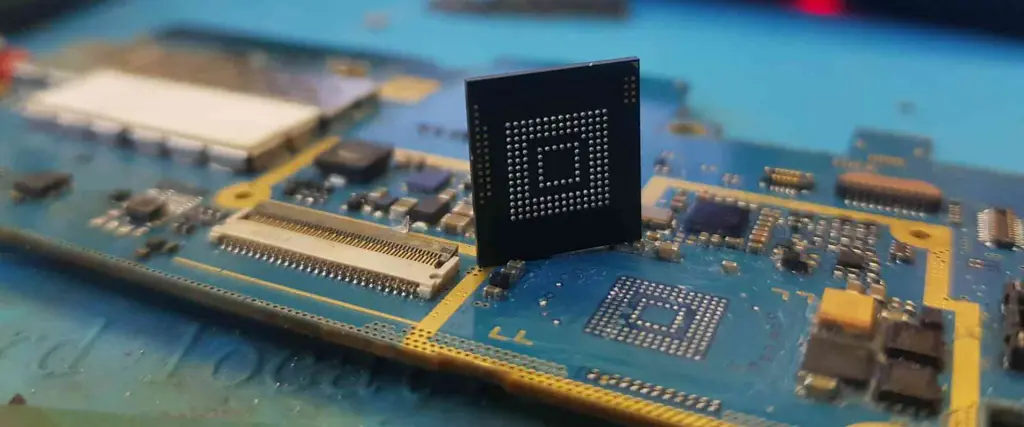
What is a BGA?
A Ball Grid Array (BGA) is a type of surface-mount packaging used for integrated circuits. Unlike traditional packages with leads around the periphery, BGAs have an array of solder balls on the bottom of the package that connect to the PCB.
Types of BGAs
There are several types of BGAs, each with its own characteristics:
- Plastic BGAs (PBGAs)
- Ceramic BGAs (CBGAs)
- Tape BGAs (TBGAs)
- Micro BGAs (μBGAs)
- Flip Chip BGAs (FCBGAs)
Advantages of BGAs
BGAs offer several advantages over other package types:
- Higher pin count in a smaller footprint
- Better electrical performance due to shorter connection lengths
- Improved thermal performance
- Self-alignment during reflow soldering
Challenges of BGAs
Despite their advantages, BGAs present some challenges:
- Difficulty in visual inspection of solder joints
- Potential for hidden solder joint failures
- More complex PCB design requirements
- Higher cost of rework and repair
Designing for Manufacturability
PCB Layout Considerations
1. Pad Design
Proper pad design is crucial for successful BGA mounting:
- Use solder mask-defined (SMD) pads for better solder joint reliability
- Consider using non-solder mask-defined (NSMD) pads for finer pitch BGAs
- Ensure proper pad size and shape based on BGA specifications
2. Trace Routing
Effective trace routing is essential for signal integrity and manufacturability:
- Use shorter traces to reduce signal degradation
- Implement proper impedance control for high-speed signals
- Consider using microvias for dense routing
3. Power and Ground Planes
Proper power and ground distribution is critical:
- Use dedicated power and ground planes
- Implement proper decoupling capacitor placement
- Consider using split planes for multiple voltage domains
Component Placement
Optimizing component placement can significantly impact manufacturability:
- Leave adequate space around BGAs for rework and inspection
- Consider thermal management when placing heat-generating components
- Group similar components together for efficient assembly
Design for Testing
Incorporating design for testing (DFT) principles can improve manufacturability:
- Implement proper test points for in-circuit testing (ICT)
- Consider boundary scan (JTAG) capabilities for BGAs
- Design for flying probe testing where applicable
Cost Optimization Strategies
BGA Selection
Choosing the right BGA package can significantly impact costs:
- Select the appropriate package size based on pin count requirements
- Consider using plastic BGAs instead of ceramic for cost-sensitive applications
- Evaluate the trade-offs between fine-pitch and standard-pitch BGAs
PCB Material Selection
The choice of PCB material affects both performance and cost:
- Use standard FR-4 material for most applications
- Consider high-performance materials only when necessary for signal integrity or thermal management
- Evaluate the cost-benefit of using multi-layer PCBs vs. increasing board size
Manufacturing Process Optimization
Optimizing the manufacturing process can lead to significant cost savings:
- Design for a single reflow process if possible
- Minimize the number of different component types
- Consider panel utilization to maximize PCB yield
Supply Chain Management
Effective supply chain management can reduce overall costs:
- Use common, widely available BGA packages
- Consider second-source options for critical components
- Evaluate the total cost of ownership, including potential rework and field failures
BGA Reliability Considerations

Thermal Management
Proper thermal management is crucial for BGA reliability:
- Implement thermal vias under BGAs when necessary
- Consider using thermal interface materials for high-power BGAs
- Design proper heat spreading in the PCB layout
Mechanical Stress Mitigation
Minimizing mechanical stress can improve BGA reliability:
- Use underfill for BGAs in high-vibration environments
- Consider the coefficient of thermal expansion (CTE) mismatch between the BGA and PCB
- Implement proper board stiffening techniques for large BGAs
Environmental Considerations
Designing for the intended operating environment is essential:
- Consider conformal coating for harsh environments
- Evaluate the need for hermetically sealed BGAs in extreme conditions
- Design for proper moisture sensitivity levels (MSL) handling
Advanced BGA Design Techniques
High-Speed Design Considerations
For high-speed applications, additional design techniques may be necessary:
- Implement proper signal integrity analysis and simulation
- Use advanced PCB stackup designs for impedance control
- Consider using buried and blind vias for improved routing
3D Packaging Techniques
Emerging 3D packaging technologies can offer new design possibilities:
- Evaluate the use of package-on-package (PoP) designs
- Consider through-silicon via (TSV) technology for advanced applications
- Explore the potential of interposer-based designs for complex systems
Design for Flexibility
Designing for flexibility can improve long-term cost-effectiveness:
- Implement modular design approaches
- Consider using programmable devices (e.g., FPGAs) in BGAs
- Design for potential future upgrades or modifications
Comparison of BGA Types
To help designers choose the most appropriate BGA type for their application, here’s a comparison table of common BGA types:
| BGA Type | Advantages | Disadvantages | Typical Applications |
| PBGA | Low cost, widely available | Limited thermal performance | Consumer electronics, low to mid-range computing |
| CBGA | Excellent thermal performance, hermetic | Higher cost, heavier | High-reliability applications, military/aerospace |
| TBGA | Very thin profile, lightweight | More expensive than PBGA, limited availability | Mobile devices, wearables |
| 渭BGA | Extremely small form factor | Challenging to manufacture and rework | Mobile devices, medical implants |
| FCBGA | Excellent electrical and thermal performance | Higher cost, more complex manufacturing |
BGA Design Checklist
To ensure a successful BGA design, consider the following checklist:
- Verify BGA package specifications and design rules
- Optimize PCB stackup for signal integrity and power distribution
- Implement proper pad and via design
- Ensure adequate thermal management
- Design for testability and inspection
- Consider manufacturing process requirements
- Evaluate cost-performance trade-offs
- Implement proper component placement and routing
- Verify signal integrity through simulation
- Consider environmental and reliability requirements
Future Trends in BGA Design
As technology continues to evolve, several trends are shaping the future of BGA design:
- Increasing pin counts and decreasing pitch sizes
- Integration of advanced packaging technologies (e.g., 2.5D and 3D ICs)
- Improved thermal management techniques
- Enhanced reliability through advanced materials and design techniques
- Greater emphasis on design for recycling and sustainability
Conclusion
Designing with BGAs for manufacturability and cost requires a careful balance of performance, reliability, and economic considerations. By understanding the unique challenges and opportunities presented by BGA technology, designers can create efficient, cost-effective, and reliable electronic products. As BGA technology continues to evolve, staying informed about the latest developments and best practices will be crucial for success in electronic design.
Frequently Asked Questions (FAQ)
- Q: What is the minimum PCB thickness recommended for BGA designs? A: The minimum PCB thickness depends on various factors, including the BGA size, pin count, and application requirements. Generally, a thickness of 0.062 inches (1.57 mm) is common for many BGA designs. However, for high-density or high-reliability applications, thicker boards may be necessary. Always consult the BGA manufacturer’s recommendations and consider the specific requirements of your design.
- Q: How can I improve the reliability of BGA solder joints? A: To improve BGA solder joint reliability, consider the following:
- Use proper pad and via designs
- Implement thermal management techniques
- Consider using underfill for high-stress environments
- Ensure proper reflow profiling during assembly
- Minimize CTE mismatch between the BGA and PCB
- Use quality solder paste and flux
- Q: What are the key considerations for routing high-speed signals with BGAs? A: When routing high-speed signals with BGAs, keep in mind:
- Maintain consistent trace widths and spacing
- Use proper impedance control techniques
- Minimize the use of vias on critical signals
- Implement proper return path design
- Consider using differential pairs for high-speed signals
- Use signal integrity simulation tools to verify design
- Q: How can I reduce the cost of BGA implementation in my design? A: To reduce BGA implementation costs:
- Choose the appropriate BGA package for your needs
- Optimize PCB layer count and material selection
- Design for standard manufacturing processes
- Minimize the use of specialized components
- Consider panel utilization during PCB layout
- Implement design for testability to reduce potential rework costs
- Q: What are the main challenges in reworking BGAs, and how can they be addressed? A: The main challenges in BGA rework include:
- Limited access to solder joints
- Risk of PCB damage during removal
- Difficulty in precise placement of new BGAs
- Potential for thermal damage to surrounding components
- Use specialized BGA rework equipment
- Implement proper thermal profiling for removal and installation
- Consider using X-ray inspection for alignment verification
- Train technicians in proper BGA rework techniques
- Design with adequate spacing around BGAs to facilitate rework