In the demanding realms of military and aerospace applications, printed circuit boards (PCBs) face extreme conditions that require exceptional performance and reliability. Thick or heavy copper PCBs have emerged as a crucial technology to meet these stringent requirements. However, designing these specialized PCBs presents unique challenges that engineers must navigate to ensure optimal functionality and durability. This article delves into the intricacies of thick copper PCB design for military and aerospace applications, exploring the key issues and potential solutions.
Understanding Thick/Heavy Copper PCBs
Definition and Characteristics
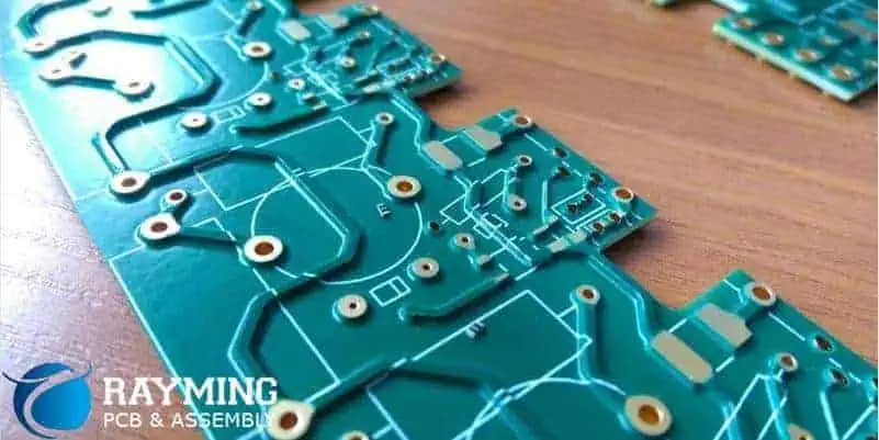
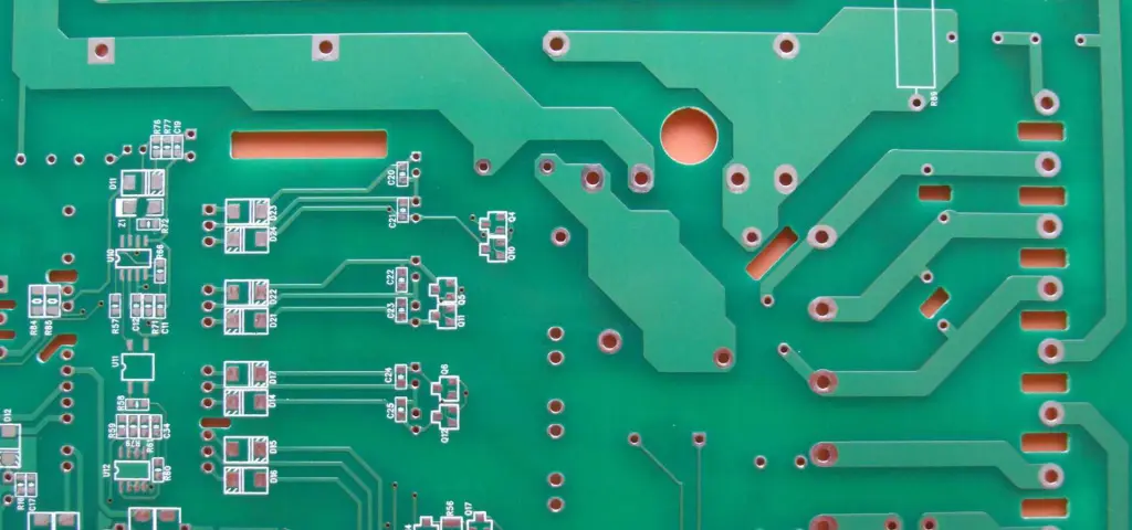
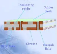
Thick or heavy copper PCBs are characterized by copper layers that exceed the standard thickness found in conventional PCBs. While standard PCBs typically use copper weights of 1 oz/ft² (35 µm) or 2 oz/ft² (70 µm), thick copper PCBs can range from 3 oz/ft² (105 µm) to as high as 20 oz/ft² (700 µm) or more.
| Copper Weight | Thickness (µm) | Typical Applications |
| 1 oz/ft² | 35 µm | Standard electronics |
| 2 oz/ft² | 70 µm | Power supplies, automotive |
| 3-4 oz/ft² | 105-140 µm | High-current devices |
| 5-10 oz/ft² | 175-350 µm | Power distribution, military/aerospace |
| >10 oz/ft² | >350 µm | Extreme high-current, specialized military/aerospace |
Advantages for Military and Aerospace Applications
- Enhanced Current Carrying Capacity: Critical for power distribution in aircraft and military vehicles.
- Improved Thermal Management: Better heat dissipation in high-power applications.
- Increased Mechanical Strength: Vital for withstanding vibration and shock in aerospace environments.
- Reduced Layer Count: Potential for more compact designs in space-constrained applications.
- Enhanced EMI Shielding: Important for protecting sensitive electronics in military equipment.
Key Design Challenges
Etching and Trace Definition
Issue Description
Etching thick copper layers presents significant challenges in maintaining precise trace definitions and achieving fine pitch designs.
Specific Challenges
- Undercut: Excessive lateral etching beneath the resist layer.
- Etch Factor: Difficulty in achieving consistent etch factors across varying trace widths.
- Minimum Trace/Space: Limitations on achievable trace width and spacing.
Design Considerations
- Adjust trace width and spacing based on copper thickness.
- Utilize advanced etching techniques (e.g., differential etching, step etching).
- Consider alternative copper patterning methods for ultra-thick copper.
| Copper Thickness | Minimum Trace Width | Minimum Space |
| 3 oz (105 µm) | 8 mil (203 µm) | 8 mil (203 µm) |
| 5 oz (175 µm) | 12 mil (305 µm) | 12 mil (305 µm) |
| 10 oz (350 µm) | 20 mil (508 µm) | 20 mil (508 µm) |
Impedance Control
Issue Description
Maintaining precise impedance control becomes more challenging with thick copper layers due to their impact on trace geometry and dielectric spacing.
Specific Challenges
- Trace Profile: Trapezoidal cross-sections affect impedance calculations.
- Dielectric Thickness: Variations due to copper thickness impact impedance.
- Surface Roughness: Increased effect on signal integrity at high frequencies.
Design Considerations
- Use advanced electromagnetic field solvers for accurate impedance modeling.
- Adjust dielectric thicknesses to compensate for copper thickness variations.
- Consider stripline configurations for critical high-speed signals.
Thermal Management
Issue Description
While thick copper improves heat dissipation, it also introduces thermal design challenges, particularly in multi-layer boards.
Specific Challenges
- Thermal Expansion Mismatch: Differential expansion between copper and substrate materials.
- Heat Distribution: Uneven heat distribution across layers.
- Thermal Vias: Design and placement for effective heat transfer.
Design Considerations
- Implement symmetric layer stacks to minimize board warpage.
- Use thermal simulation tools to optimize heat distribution.
- Design efficient thermal via patterns for critical components.
Drilling and Via Formation
Issue Description
Drilling through thick copper layers and forming reliable vias present significant manufacturing challenges.
Specific Challenges
- Drill Bit Wear: Rapid wear leading to poor hole quality.
- Aspect Ratio Limitations: Difficulties in achieving high aspect ratio holes.
- Plating Uniformity: Challenges in achieving uniform plating in high aspect ratio vias.
Design Considerations
- Adjust via sizes and aspect ratios based on board thickness and copper weight.
- Consider stacked or staggered via designs for thick boards.
- Implement back-drilling for improved signal integrity in high-speed designs.
| Board Thickness | Max Aspect Ratio | Min Via Diameter |
| < 62 mils | 8:01 | 8 mil (203 µm) |
| 63-93 mils | 10:01 | 10 mil (254 µm) |
| 94-125 mils | 12:01 | 12 mil (305 µm) |
EMI/EMC Considerations
Issue Description
While thick copper can enhance EMI shielding, it also introduces challenges in managing electromagnetic compatibility (EMC) in complex military and aerospace systems.
Specific Challenges
- Resonant Cavities: Thick copper planes can create unintended resonant cavities.
- Skin Effect: Increased impact on high-frequency signal transmission.
- Crosstalk: Potential for increased crosstalk due to larger conductor surfaces.
Design Considerations
- Implement proper grounding and shielding strategies.
- Use electromagnetic simulation tools to analyze and mitigate EMI issues.
- Consider embedded shielding layers for critical circuits.
Manufacturing and Assembly
Issue Description
Thick copper PCBs require specialized manufacturing processes and present unique assembly challenges.
Specific Challenges
- Layer Registration: Maintaining accurate alignment of thick copper layers.
- Pressing and Lamination: Achieving uniform pressure and bond strength.
- Solderability: Ensuring reliable solder joints on thick copper pads.
Design Considerations
- Design with manufacturing tolerances appropriate for thick copper processes.
- Specify appropriate surface finishes for reliable soldering.
- Consider testability and implement suitable test points and strategies.
Advanced Design Techniques
3D Modeling and Simulation
Utilizing advanced 3D modeling and simulation tools is crucial for optimizing thick copper PCB designs:
- Electromagnetic Simulation:
- Full-wave 3D EM simulations for accurate signal integrity analysis.
- Optimization of power distribution networks.
- Thermal Modeling:
- Detailed thermal simulations to identify and mitigate hotspots.
- Analysis of thermal expansion effects on board reliability.
- Mechanical Stress Analysis:
- Finite Element Analysis (FEA) to predict board warpage and stress points.
- Optimization of layer stack-ups for minimal thermal and mechanical stress.
Novel Copper Patterning Techniques
Exploring advanced copper patterning methods to overcome traditional etching limitations:
- Semi-Additive Process (SAP):
- Enables finer lines and spaces in thick copper layers.
- Improved control over trace profiles.
- Modified Semi-Additive Process (mSAP):
- Further refinement of SAP for even finer feature sizes.
- Potential for mixed thickness copper on the same layer.
- Laser Direct Structuring (LDS):
- Precision patterning of complex 3D circuits.
- Potential for integration of electrical and mechanical functions.
Embedded Components
Integrating embedded components to optimize space and improve performance:
- Embedded Passives:
- Resistors and capacitors embedded within the PCB layers.
- Improved signal integrity and reduced board size.
- Embedded Actives:
- Integration of semiconductor devices within the PCB structure.
- Enhanced thermal management and reduced interconnect parasitics.
- Cavity Designs:
- Creation of recessed areas for component placement.
- Improved planarity for large BGAs and other surface mount devices.
Advanced Materials
Incorporating specialized materials to enhance performance and reliability:
| Material Type | Properties | Benefits for Thick Copper PCBs |
| High Tg Laminates | Glass transition temperature >170°C | Improved thermal stability, reduced warpage |
| Low CTE Materials | Coefficient of Thermal Expansion <10 ppm/°C | Better matching with copper, reduced stress |
| Ceramic-Filled PTFE | Low dielectric constant, stable at high frequencies | Improved signal integrity for RF/microwave applications |
| Polyimide | High temperature resistance, low outgassing | Suitable for extrem |
Hybrid Construction Techniques
Combining different PCB technologies to optimize performance:
- Rigid-Flex Integration:
- Incorporation of flexible circuits with thick copper rigid sections.
- Improved reliability in high-vibration environments.
- Mixed Dielectric Stack-ups:
- Utilization of different dielectric materials in the layer stack.
- Optimization of electrical and thermal properties.
- Selective Copper Thickness:
- Varying copper thickness across the board or within layers.
- Balancing high-current capacity with fine-pitch routing requirements.
Design for Reliability and Qualification
Environmental Stress Testing
Implementing rigorous testing protocols to ensure reliability in extreme conditions:
- Thermal Cycling:
- Test temperature range: -65°C to +150°C (or application-specific).
- Number of cycles based on mission profile (e.g., 500-1000 cycles).
- Vibration Testing:
- Random vibration profiles simulating launch and flight conditions.
- Typical frequency range: 20 Hz to 2000 Hz.
- Shock Testing:
- Pyrotechnic shock simulation for space applications.
- Mechanical shock for ground and aviation applications.
- Humidity and Salt Fog Exposure:
- Testing for corrosion resistance and insulation integrity.
- Typical conditions: 85% RH at 85°C for 1000 hours.
Reliability Modeling and Prediction
Utilizing advanced modeling techniques to predict long-term reliability:
- Physics of Failure (PoF) Approach:
- Modeling of failure mechanisms specific to thick copper PCBs.
- Prediction of time-to-failure under various stress conditions.
- Accelerated Life Testing:
- Development of acceleration factors for various stress conditions.
- Extrapolation of test results to predict service life.
- Finite Element Analysis (FEA):
- Detailed modeling of thermal and mechanical stresses.
- Identification of potential failure points for design optimization.
Qualification Standards
Adhering to stringent military and aerospace qualification standards:
| Standard | Description | Key Requirements for Thick Copper PCBs |
| MIL-PRF-31032 | Performance Specification for Printed Circuit Board | Specific requirements for high-reliability PCBs |
| MIL-PRF-55110 | General Specification for Printed Wiring Board | Qualification and performance requirements |
| RTCA DO-254 | Design Assurance Guidance for Airborne Electronic Hardware | Design assurance levels for avionics |
| NASA-STD-8739.1 | Workmanship Standard for Polymeric Application on Electronic Assemblie |
Design for Manufacturability (DFM) and Testability (DFT)
Implementing strategies to ensure manufacturable and testable designs:
- DFM Considerations:
- Adherence to manufacturer-specific design rules for thick copper.
- Implementation of copper thieving and balancing techniques.
- Consideration of etching compensation factors.
- DFT Strategies:
- Implementation of robust test point strategies.
- Design for In-Circuit Test (ICT) and Flying Probe compatibility.
- Incorporation of Built-In Self-Test (BIST) capabilities where applicable.
Future Trends and Innovations
Advanced Copper Deposition Technologies
Emerging technologies for more precise and efficient copper deposition:
- Pulse Plating:
- Improved control over copper grain structure.
- Potential for reduced internal stress in thick copper layers.
- Periodic Pulse Reverse (PPR) Plating:
- Enhanced uniformity in high aspect ratio vias.
- Improved throwing power for complex geometries.
- Direct Copper Laser Sintering:
- Additive manufacturing approach for 3D copper structures.
- Potential for highly customized power distribution networks.
Integration with Additive Manufacturing
Exploring synergies between PCB technology and 3D printing:
- 3D Printed Electronics:
- Direct printing of conductive traces and components.
- Potential for truly three-dimensional circuit designs.
- Hybrid PCB-AM Processes:
- Combination of traditional PCB fabrication with additive techniques.
- Enhanced design freedom for complex geometries.
Advanced Thermal Management Solutions
Novel approaches to managing heat in high-power designs:
- Embedded Heat Pipes:
- Integration of miniature heat pipes within PCB layers.
- Efficient heat spreading for localized high-power components.
- Phase Change Materials (PCMs):
- Incorporation of PCMs for thermal energy storage and management.
- Potential for improved thermal stability in pulsed-power applications.
- Graphene-Enhanced Thermal Management:
- Utilization of graphene’s superior thermal conductivity.
- Potential for ultra-thin, high-efficiency thermal management layers.
AI-Driven Design Optimization
Leveraging artificial intelligence for advanced PCB design:
- Machine Learning for DFM:
- AI-driven optimization of design rules for thick copper PCBs.
- Continuous improvement based on manufacturing feedback.
- Generative Design for Thermal Management:
- AI-generated optimized thermal management structures.
- Potential for novel, highly efficient cooling solutions.
- Predictive Reliability Modeling:
- AI-enhanced prediction of long-term reliability.
- Integration of vast datasets for more accurate life predictions.
Conclusion
Designing thick/heavy copper PCBs for military and aerospace applications presents a unique set of challenges that require careful consideration and advanced engineering techniques. From managing complex etching processes to ensuring reliable performance in extreme environments, engineers must navigate a multitude of design issues.
By leveraging advanced simulation tools, novel manufacturing techniques, and emerging technologies, it is possible to create robust, high-performance PCBs that meet the stringent requirements of military and aerospace applications. As the field continues to evolve, ongoing research and development in areas such as advanced materials, additive manufacturing, and AI-driven design optimization promise to further enhance the capabilities and reliability of thick copper PCBs.
The successful implementation of these advanced PCB designs plays a crucial role in enabling next-generation military and aerospace systems, from high-power radar systems to space-based communications platforms. As technology continues to advance, the importance of addressing these design challenges will only grow, driving further innovation in the field of PCB design and manufacturing.