Printed circuit boards (PCBs) rely on vias—tiny conductive pathways that transmit signals between layers. During manufacturing, a copper layer is deposited onto the substrate, forming both the conductive traces and the plated through-hole (PTH) walls that interconnect layers. While standard plated vias are sufficient for many applications, advanced designs often demand copper-filled vias for superior performance.
To create a copper-filled via, manufacturers first fill the via with an epoxy resin, then electroplate it with pure copper. This process increases fabrication costs but unlocks unique benefits:
- Higher current-carrying capacity (reduced resistance vs. hollow or non-copper fills).
- Improved thermal conductivity, critical for power electronics and high-temperature applications.
- Enhanced structural integrity, minimizing risks of void formation or cracking during thermal cycling.

Unlike alternative conductive fills (e.g., silver paste), copper-filled vias offer lower impedance and better high-frequency performance, making them ideal for:
- High-power PCBs (e.g., automotive, industrial).
- HDI designs requiring microvias.
- RF/microwave circuits where signal integrity is paramount.
This guide explores the key advantages of copper-filled vias and how to leverage them in your PCB designs.
Understanding Copper Filled Vias
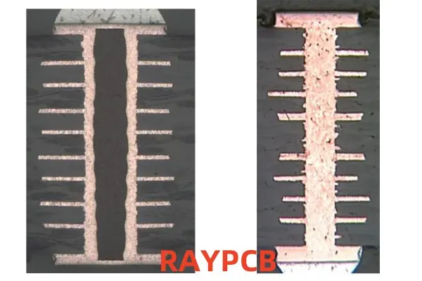
Copper filled vias are a type of plated through-hole (PTH) in a printed circuit board that has been completely filled with copper. Unlike traditional vias that are hollow, copper filled vias are solid, providing a continuous path for electrical signals and heat dissipation.
Key Features of Copper Filled Vias
- Solid Construction: Filled entirely with copper, eliminating air gaps.
- Enhanced Conductivity: Offers superior electrical performance compared to hollow vias.
- Improved Thermal Management: Facilitates better heat dissipation.
- Increased Reliability: Reduces the risk of via failure due to thermal stress or mechanical strain.
Types of Copper Filled Vias
- Through-Hole Copper Filled Vias: Extend through all layers of the PCB.
- Blind Copper Filled Vias: Connect an outer layer to one or more inner layers, but not through the entire board.
- Buried Copper Filled Vias: Connect inner layers without extending to the outer layers.
Read more about:
Via Filling Process
The process of filling vias with copper or other materials is a critical step in advanced PCB manufacturing. Let’s explore the various methods used for via filling.
1. Conductive Via Filling
Conductive via filling involves using electrically conductive materials to fill the vias. Copper is the most common material used due to its excellent conductivity and compatibility with PCB manufacturing processes.
Process Steps for Copper Filled Vias:
- Via Drilling: Creating the initial hole in the PCB.
- Cleaning: Removing any debris from the drilling process.
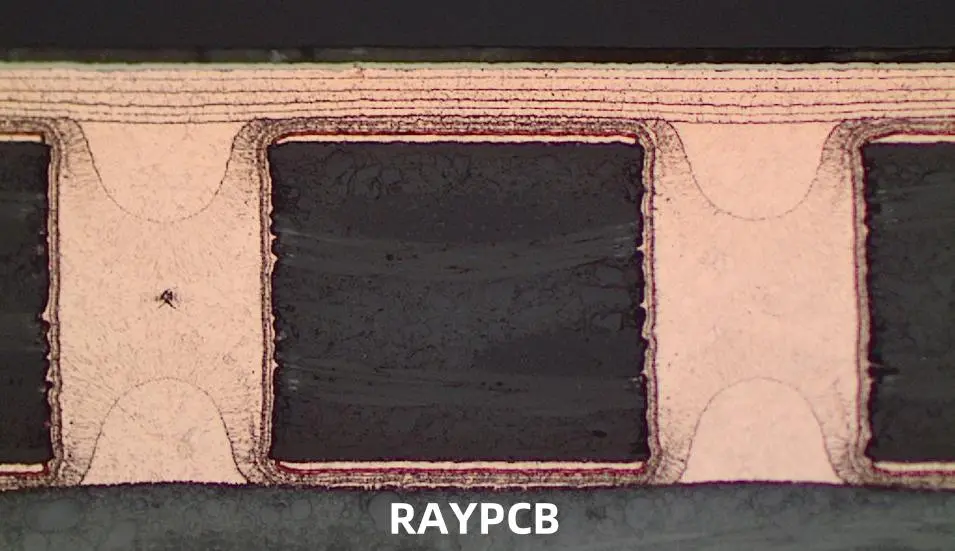
- Electroplating: Depositing a thin layer of copper on the via walls.
- Copper Filling: Using electroplating or paste filling techniques to completely fill the via with copper.
- Planarization: Removing excess copper to create a smooth surface.
2. Non-Conductive Via Filling
Non-conductive via filling uses insulating materials, typically epoxy resins, to fill the vias. This method is often used when electrical conductivity through the via is not required.
Applications of Non-Conductive Filled Vias:
- Improving board planarity for surface mount assembly.
- Enhancing the structural integrity of the PCB.
- Creating a smooth surface for legend printing or solder mask application.
3. Copper-Plated Shut Filled Vias
Copper-plated shut vias are a variation of copper filled vias where the via is gradually plated shut rather than being completely filled.
Characteristics of Copper-Plated Shut Vias:
- Process: Involves extended electroplating to close the via opening.
- Structure: Results in a via that is mostly hollow but sealed at both ends.
- Applications: Used in situations where full copper filling is not necessary but via sealing is required.
4. Epoxy Filled Vias
Epoxy filled vias use a non-conductive epoxy resin to fill the via hole. This method is often used in conjunction with copper plating for specific applications.
Benefits of Epoxy Filled Vias:
- Cost-Effective: Generally less expensive than full copper filling.
- Planar Surface: Provides a smooth surface for component mounting.
- Structural Support: Enhances the mechanical strength of the PCB.
5. Gold Filled Via
Gold filled vias are a specialized type of conductive via filling used in high-reliability applications.
Features of Gold Filled Vias:
- Superior Conductivity: Gold offers excellent electrical performance.
- Corrosion Resistance: Gold’s inert nature prevents oxidation and corrosion.
- High-Reliability Applications: Often used in aerospace and medical devices.
Benefits of Copper Filled Vias
Copper filled vias offer numerous advantages over traditional hollow vias, making them increasingly popular in high-performance PCB designs.
1. Enhanced Electrical Performance
- Lower Resistance: Solid copper provides a more conductive path for electrical signals.
- Reduced Signal Loss: Minimizes signal degradation in high-frequency applications.
- Improved Signal Integrity: Reduces electromagnetic interference (EMI) and crosstalk.
2. Superior Thermal Management
- Efficient Heat Dissipation: Copper’s high thermal conductivity helps in removing heat from components.
- Thermal Via Applications: Ideal for creating thermal vias under high-power components.
3. Increased Reliability
- Mechanical Strength: Solid structure improves the overall durability of the PCB.
- Resistance to Thermal Stress: Better withstands temperature fluctuations and thermal cycling.
- Reduced Risk of Failure: Eliminates issues related to hollow via failures, such as trapped chemicals or air bubbles.
4. Design Flexibility
- Higher Current Capacity: Allows for thinner traces while maintaining current-carrying capability.
- Space Saving: Enables more compact designs by reducing the need for multiple vias.
5. Manufacturing Benefits
- Improved Yields: Reduces issues related to via plating inconsistencies.
- Enhanced Planarity: Creates a smoother surface for component mounting and assembly.
Filled Via vs. Plated Through Hole Applications

While copper filled vias and traditional plated through holes (PTHs) serve similar purposes, they have distinct characteristics that make them suitable for different applications.
Copper Filled Vias:
- High-Density Designs: Ideal for HDI boards where space is at a premium.
- High-Frequency Applications: Better signal integrity in RF and high-speed digital circuits.
- Thermal Management: Superior heat dissipation for power electronics.
Plated Through Holes:
- Cost-Effective: Generally less expensive for simpler board designs.
- Ease of Manufacturing: Simpler process for basic PCB production.
- Through-Board Connections: Effective for connecting multiple layers in thicker boards.
Similarities and Differences Between Copper and Epoxy Filled Vias
Understanding the similarities and differences between copper and epoxy filled vias can help in choosing the right option for specific PCB applications.
Similarities:
- Improved Planarity: Both provide a smooth surface for component mounting.
- Enhanced Structural Integrity: Increase the overall strength of the PCB.
- Via Sealing: Both methods effectively seal the via, preventing ingress of contaminants.
Differences:
Copper Filled Vias:
- Conductivity: Electrically conductive throughout the via.
- Thermal Performance: Superior heat dissipation.
- Cost: Generally more expensive due to the copper filling process.
Epoxy Filled Vias:
- Insulation: Electrically insulating, useful for certain design requirements.
- Cost: Typically less expensive than copper filling.
- Thermal Properties: Lower thermal conductivity compared to copper.
Copper Filled Via PCB Applications
Copper filled vias find applications in a wide range of high-performance electronic products and industries.
1. Aerospace and Defense
- Satellite Communications: High-reliability boards for space applications.
- Radar Systems: High-frequency PCBs with excellent signal integrity.
- Avionics: Rugged boards capable of withstanding extreme conditions.
2. Telecommunications
- 5G Infrastructure: High-speed, high-density boards for network equipment.
- Optical Networking: PCBs for fiber optic communication systems.
3. Consumer Electronics
- Smartphones: Compact, multi-layer boards with high component density.
- Wearable Devices: Thin, flexible PCBs with efficient thermal management.
4. Automotive Electronics
- Advanced Driver Assistance Systems (ADAS): High-reliability boards for safety-critical applications.
- Electric Vehicle Control Systems: Power electronics with superior thermal management.
5. Medical Devices
- Implantable Devices: High-reliability, biocompatible PCBs.
- Diagnostic Equipment: High-performance boards for medical imaging systems.
6. High-Performance Computing
- Data Centers: Servers and networking equipment requiring high-speed signal transmission.
- Artificial Intelligence Hardware: Dense, high-performance boards for AI accelerators.
Conclusion: The Future of Copper Filled Vias in PCB Technology
As the electronics industry continues to push the boundaries of performance and miniaturization, copper filled vias will play an increasingly crucial role in PCB design and manufacturing. Their ability to enhance electrical performance, improve thermal management, and increase reliability makes them indispensable for cutting-edge electronic products.
Looking ahead, we can expect to see further innovations in copper filling techniques, potentially leading to even smaller via sizes and higher aspect ratios. Additionally, the integration of copper filled vias with other advanced PCB technologies, such as embedded components and 3D printing, may open up new possibilities in electronic design.
For PCB designers and manufacturers, staying abreast of developments in copper filled via technology will be essential for creating the next generation of high-performance, reliable electronic devices. As this technology continues to evolve, it will undoubtedly enable new advancements across various industries, from telecommunications and aerospace to medical devices and beyond.