The XQ2V1000 is a defense-grade Field-Programmable Gate Array (FPGA) from Xilinx’s QPro Virtex-II Military QML Platform FPGA family. Designed specifically for high-reliability aerospace and defense applications, the XQ2V1000 offers 1 million system gates and combines robust performance with military-grade reliability. This device leverages advanced 0.15μm/0.12μm CMOS 8-layer metal process technology to deliver high-speed operation with optimized power consumption for mission-critical systems.
The XQ2V1000 sits within Xilinx’s QPro Virtex-II platform FPGA family, which was introduced in January 2001 and represented a significant advancement in FPGA technology for military and aerospace applications. With its 1 million system gate capacity, the XQ2V1000 provides a powerful and flexible platform for implementing complex digital systems in harsh environments. The “XQ” prefix designates its military qualification, while the “2V1000” indicates its position in the Virtex-II family with approximately 1 million system gates.
Powered By EmbedPress
Key Features
Logic Resources
System Gates: 1 million system gates
Configurable Logic Blocks (CLBs): Arranged in rows and columns
Slices: Each CLB contains two slices, with each slice containing two function generators
Look-Up Tables: Four-input LUTs for implementing any four-input Boolean function
Flip-Flops: Storage elements for sequential logic
Block RAM: Dual-port 18Kb blocks with configurable width and depth
Distributed RAM: Flexible memory implementation using CLB resources
Processing Capabilities
Clock Management: Digital Clock Manager (DCM) for clock distribution and phase control
The XQ2V1000 features a coarse-grained architecture consisting of Configurable Logic Blocks (CLBs) arranged in rows and columns. Each CLB consists of four logic cells arranged in two slices. Each slice contains:
Two function generators (implemented as 4-input LUTs)
Two storage elements (flip-flops)
Arithmetic logic gates
Multiplexers
Fast carry look-ahead chain
Horizontal cascade capability
Memory Resources
Memory in the XQ2V1000 is implemented through a hierarchy of resources:
Block SelectRAM: 2.5Mb of dual-port RAM in 18Kb blocks
Distributed SelectRAM: Up to 1Mb of memory implemented in CLBs
Flexible memory configuration options for width and depth
Clock Management
The XQ2V1000 includes Digital Clock Manager (DCM) blocks that provide:
Clock distribution with minimal skew
Frequency synthesis
Phase shifting
Domain crossing capabilities
Input/Output Features
The device offers versatile I/O capabilities:
Multiple I/O banks with independent voltage standards
Support for numerous single-ended standards (LVTTL, LVCMOS, etc.)
Support for differential standards (LVDS, HSTL, etc.)
Dedicated DDR support for high-bandwidth memory interfaces
System Generator for DSP for algorithm implementation
IP cores for accelerated design implementation
Ordering Information
When ordering the XQ2V1000 device, the complete part number follows this format: XQ2V1000-[Speed Grade][Package][Temperature Grade]
Example: XQ2V1000-4BG575N
XQ2V1000: Device name
4: Speed grade (-4, -5, or -6 available)
BG575: 575-pin Ball Grid Array package
N: Industrial temperature grade (or M for military)
Conclusion
The XQ2V1000 provides a robust platform for implementing complex digital systems in demanding military and aerospace applications. With its million-gate capacity, versatile I/O capabilities, and military qualification, this defense-grade FPGA delivers reliable performance for mission-critical systems. As part of Xilinx’s QPro Virtex-II family, the XQ2V1000 represents a mature technology with established reliability and well-documented design methodologies, making it suitable for long-lifecycle defense and aerospace programs where reliability is paramount.
For complete specifications and detailed information, please refer to the official Xilinx (now AMD) documentation including the QPro Virtex-II Military QML Platform FPGAs Datasheet and the Virtex-II Platform FPGA User Guide.
The XQ6SLX150 is a high-performance defense-grade Field-Programmable Gate Array (FPGA) from the Xilinx Spartan-6Q family, designed specifically for mission-critical applications in aerospace and defense sectors. Built on a mature 45nm low-power copper process technology, this device offers an optimal balance of cost, power efficiency, and performance while meeting the stringent requirements of military and defense applications.
Powered By EmbedPress
Device Overview
The XQ6SLX150 represents the highest-density device in the defense-grade Spartan-6Q FPGA family with 147,443 logic cells, making it ideal for complex digital systems in rugged environments. This device undergoes additional screening and qualification testing beyond commercial variants, ensuring reliability in mission-critical applications. The “XQ” prefix designates its defense-grade qualification, while the “SLX150” indicates its position as the highest capacity device in the Spartan-6 LX (logic-optimized) family.
When ordering the XQ6SLX150 device, the complete part number follows this format: XQ6SLX150-[Speed Grade][Package][Temperature Grade]
Example: XQ6SLX150-2CSG484Q
XQ6SLX150: Device name
2: Speed grade (-2Q or -3Q available)
CSG484: Package type and pin count
Q: Extended temperature range qualification
Conclusion
The XQ6SLX150 delivers high-performance FPGA capabilities for defense applications, combining Xilinx’s proven Spartan-6 architecture with extended reliability features required for mission-critical systems. With its balance of logic density, processing capability, and power efficiency, this defense-grade FPGA provides a secure and reliable platform for advanced military and aerospace applications where failure is not an option.
For complete specifications and detailed information, please refer to the official Xilinx/AMD documentation including the Spartan-6Q Family Overview (DS172) and the Spartan-6 FPGA Data Sheet: DC and Switching Characteristics (DS162).
In the rapidly evolving landscape of defense and aerospace electronics, Field Programmable Gate Arrays (FPGAs) serve as crucial components that enable mission-critical systems to operate with exceptional reliability, performance, and security. The XQ6SLX75T-2FG484Q, manufactured by Xilinx (now part of AMD), represents one of the most significant technological advancements in this domain. This defense-grade FPGA belongs to the renowned Spartan-6Q family, specifically engineered to meet the stringent requirements of military communications, avionics, missile systems, and space applications.
The XQ6SLX75T-2FG484Q is built on a 45nm process technology, offering an optimal balance between power efficiency and computational performance. At its core, this FPGA features 74,637 logic cells arranged in approximately 11,662 logic blocks, providing substantial resources for implementing complex digital systems. The device is packaged in a 484-pin FBGA (Fine-pitch Ball Grid Array) configuration, facilitating integration into space-constrained defense hardware.
Key technical specifications include:
Logic Resources: 74,637 logic cells
Package Type: 484-pin FBGA (FG484Q)
Speed Grade: -2 (moderate performance grade)
Core Voltage: 1.14V to 1.26V (nominal 1.2V)
Temperature Range: Extended military temperature range
Manufacturing Process: 45nm CMOS technology
Memory Capacity: Approximately 3.17Mb of embedded block RAM
DSP Resources: Advanced DSP48A1 slices for digital signal processing
I/O Capability: Up to 280 user-configurable I/O pins
The “XQ” prefix in the part number specifically denotes the defense-grade qualification, indicating enhanced reliability testing and ruggedization compared to commercial variants. The “6SLX75T” portion identifies it as a Spartan-6 LXT device with approximately 75,000 logic cells and transceiver capabilities.
What truly distinguishes the XQ6SLX75T-2FG484Q from commercial FPGAs is its defense-grade characteristics. This device incorporates:
Information Assurance (IA): The FPGA supports third-generation Information Assurance capabilities, making it suitable for single-chip cryptographic implementations in Type-1 secure communications systems.
Anti-Tamper (AT) Protection: In compliance with DoD 5000 series requirements, the device features robust anti-tamper mechanisms to protect sensitive intellectual property and prevent unauthorized access or reverse engineering.
Environmental Robustness: Qualified for extended temperature operation across industrial (I-grade) and military (Q-grade) temperature ranges, ensuring reliable performance in extreme environments from -40°C to +125°C.
Enhanced Quality Assurance: Manufactured with stringent quality controls, each unit undergoes comprehensive testing to meet military and aerospace quality standards.
Application Domains
The XQ6SLX75T-2FG484Q finds critical applications across various defense and aerospace sectors:
Military Communications (MILCOM)
The device serves as the foundation for secure tactical communication systems, including:
Type-1 cryptographic handheld radios
Multi-waveform software-defined radios
Battlefield communication networks
Secure data transmission systems
Missiles & Munitions
Its compact form factor and robust operation make it ideal for:
As part of the Spartan-6 LXT subfamily, the XQ6SLX75T-2FG484Q incorporates high-speed serial transceivers that set it apart from standard LX devices. These GTP transceivers support data rates up to 3.125 Gbps, enabling implementation of numerous high-speed protocols:
Gigabit Ethernet
PCI Express (Gen1)
XAUI
Aurora
DisplayPort
CPRI (Common Public Radio Interface)
OBSAI (Open Base Station Architecture Initiative)
This exceptional connectivity makes the device particularly valuable for applications requiring high-bandwidth data transfer in constrained environments.
Security and Anti-Tamper Features
In the defense sector, protecting sensitive technologies from unauthorized access or exploitation is paramount. The XQ6SLX75T-2FG484Q incorporates multiple security features:
Bitstream Encryption: Utilizing advanced encryption standards to protect configuration data
Physical Security Measures: Designed to resist various side-channel attacks
Anti-Reverse Engineering Features: Physical and logical countermeasures against tampering
These security features make the device suitable for systems requiring the highest levels of information assurance and protection against sophisticated adversaries.
Design and Development Environment
The XQ6SLX75T-2FG484Q is supported by Xilinx‘s ISE Design Suite, providing a comprehensive development environment for defense applications. This software platform offers:
Compatibility with defense industry standard design flows
The availability of pre-qualified IP cores significantly accelerates the development of complex defense systems while ensuring compliance with military standards.
Reliability and Radiation Effects
While not specifically designed as a radiation-hardened device like the dedicated space-grade Virtex series, the XQ6SLX75T-2FG484Q offers improved radiation tolerance compared to commercial components. This makes it suitable for certain aerospace applications with moderate radiation environments.
The device features:
Enhanced Total Ionizing Dose (TID) tolerance
Improved Single Event Effect (SEE) resistance
Mitigation techniques for Single Event Upsets (SEUs)
Qualification for various defense reliability standards
Comparison with Alternative Technologies
When compared to other technologies used in defense applications, the XQ6SLX75T-2FG484Q offers several advantages:
Technology
Flexibility
Performance
Power Efficiency
Security
Development Time
XQ6SLX75T-2FG484Q
Very High
High
Moderate
Very High
Moderate
ASICs
Very Low
Very High
Very High
High
Very Long
Commercial FPGAs
High
High
Moderate
Low
Short
Microprocessors
Moderate
Moderate
Moderate
Moderate
Short
The defense-grade FPGA strikes an optimal balance between the flexibility of programmable logic and the security requirements of defense applications, offering a compelling alternative to custom ASICs for many military systems.
Supply Chain and Lifecycle Management
For defense contractors, component lifecycle and supply chain security are critical considerations. The XQ6SLX75T-2FG484Q is manufactured under Xilinx’s (now AMD’s) rigorous supply chain security protocols, ensuring:
Extended product lifecycle support
Stringent component traceability
Protection against counterfeit components
Compliance with defense procurement requirements
Long-term availability guarantees
These factors make the device particularly valuable for defense programs with extended operational lifespans and strict security requirements.
Conclusion: Strategic Importance in Defense Electronics
The XQ6SLX75T-2FG484Q represents a critical enabling technology for modern defense systems, bridging the gap between commercial electronics and specialized military requirements. Its combination of high performance, enhanced security features, and defense qualification makes it an essential component in maintaining technological superiority in defense applications.
As warfare continues to evolve toward more digitally integrated and network-centric paradigms, FPGAs like the XQ6SLX75T-2FG484Q will play an increasingly vital role in enabling the rapid development and deployment of sophisticated electronic warfare, communications, and weapons systems. The device’s programmable nature also provides future-proofing capabilities, allowing defense systems to adapt to emerging threats and requirements through field updates rather than complete hardware redesigns.
In the landscape of defense electronics, the XQ6SLX75T-2FG484Q stands as a testament to the critical intersection of advanced semiconductor technology and national security requirements—embodying the sophisticated capabilities required to maintain technological superiority in increasingly complex operational environments.
In the evolving landscape of programmable logic devices, Field-Programmable Gate Arrays (FPGAs) have secured a critical position in modern electronic design. The XQ6SLX75-2FG484I, part of Xilinx‘s (now AMD’s) renowned Spartan-6 FPGA family, represents a significant offering in defense-grade programmable solutions. This article provides a detailed examination of this component, exploring its specifications, applications, advantages, and its ranking among similar devices in the market.
6SLX75: Part of the Spartan-6 LX family with 74,637 logic cells
-2: Speed grade (with -3 being the highest performance)
FG484: FBGA package with 484 pins
I: Industrial temperature range
Technical Specifications
The XQ6SLX75-2FG484I is manufactured using a mature 45nm low-power copper process technology that balances cost, power efficiency, and performance. As a defense-grade variant (denoted by the “XQ” prefix), it undergoes additional screening and qualification testing for use in mission-critical applications.
Core Specifications
Logic Cells: 74,637
Operating Frequency: Up to 667MHz
Technology: 45nm CMOS
Package: 484-pin FBGA (23 x 23mm, 1mm pitch)
Temperature Range: Industrial (-40°C to +100°C)
Core Voltage: 1.2V
Speed Grade: -2 (middle performance tier)
Architecture Features
Dual-register 6-input lookup table (LUT) logic
18 Kb (2 x 9 Kb) block RAMs
Second generation DSP48A1 slices for signal processing
Enhanced mixed-mode clock management blocks
SelectIO technology for versatile I/O capabilities
Advanced system-level power management modes
Enhanced IP security with AES and Device DNA protection
Signal Processing: Real-time data acquisition and processing in harsh environments
Protocol Bridging: Connecting legacy systems with modern interfaces
Secure Communications: Encrypted data transmission systems
The device excels in applications requiring the balance of performance, power efficiency, and reliability in challenging operational environments.
Performance Characteristics
The -2 speed grade of the XQ6SLX75-2FG484I positions it in the mid-range of performance for the Spartan-6 family. While not as fast as the -3 speed grade, it offers an optimal balance between performance and power consumption.
I/O Capabilities
Support for over 40 I/O standards
High logic-to-pin ratio
Compatibility with 33 MHz, 32-bit and 64-bit PCI specifications
Support for interface protocols including Ethernet, UART, SPI, and more
Power Management
The device incorporates advanced power management technologies:
Multiple power domains
Flexible shutdown of unused blocks
Power-optimized architecture that reduces static and dynamic power consumption
Development Environment
Development for the XQ6SLX75-2FG484I is supported through:
ISE Design Suite (rather than the newer Vivado, which supports 7-series and later)
ChipScope Pro for debugging
System Generator for DSP design
EDK (Embedded Development Kit) for MicroBlaze soft processor implementation
Market Position and Ranking
When ranking the XQ6SLX75-2FG484I against similar FPGAs, several factors must be considered:
Performance Ranking (1-10, with 10 being highest)
Raw Processing Power: 7/10 – Good performance with 74,637 logic cells
Speed: 6/10 – The -2 speed grade offers moderate performance
Energy Efficiency: 8/10 – 45nm technology provides good power characteristics
I/O Capability: 7/10 – Versatile I/O options with high pin count
Cost-Performance Ratio: 7/10 – Higher cost due to defense-grade qualification
Development Ecosystem: 6/10 – Mature but older ISE platform
Security Features: 8/10 – Enhanced with AES and Device DNA protection
Overall Ranking: 7.5/10
The XQ6SLX75-2FG484I ranks highly among defense-grade FPGAs in its generation, offering an excellent balance of performance, reliability, and power efficiency. However, newer FPGA families like the 7-Series (Artix, Kintex) or UltraScale provide better performance and lower power consumption with enhanced features.
Comparative Analysis
Compared to its commercial counterpart (XC6SLX75-2FG484I), the defense-grade XQ variant offers:
Extended temperature range qualification
Enhanced reliability testing
Longer lifecycle support
Higher guaranteed MTBF (Mean Time Between Failures)
UltraScale architecture for higher performance requirements
Cost Considerations
The XQ6SLX75-2FG484I commands a premium price due to its defense-grade qualification. Typical pricing ranges from $150-$160 per unit in large quantities (1500+), making it significantly more expensive than commercial equivalents. This price point reflects the additional testing, quality control, and guaranteed lifecycle support that defense applications require.
Conclusion
The XQ6SLX75-2FG484I represents a robust, reliable solution for defense and high-reliability applications. While newer FPGA families offer improved performance metrics, the Spartan-6 defense-grade devices continue to serve critical applications where proven reliability and long-term support are essential. With its balanced feature set, extensive qualification, and mature development environment, this FPGA remains a viable option for new designs in the defense sector and for maintaining legacy systems.
For mission-critical applications requiring a balance of performance, power efficiency, and proven reliability, the XQ6SLX75-2FG484I earns its 7.5/10 ranking as a dependable, defense-grade programmable logic solution.
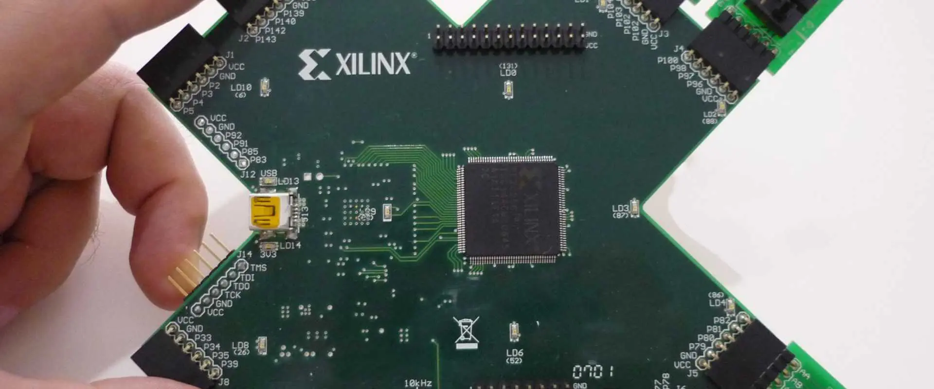
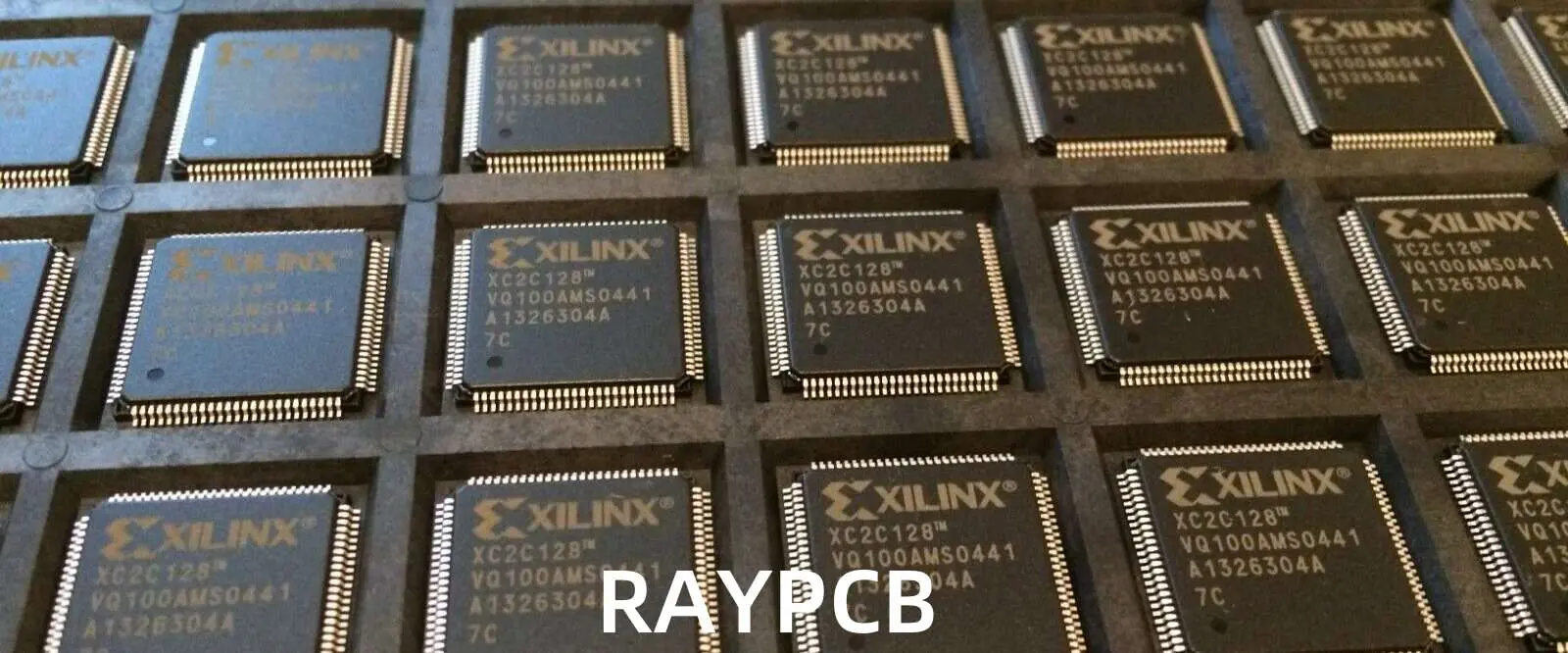
In the rapidly evolving world of digital electronics design, programmable logic devices have become essential components for engineers seeking flexibility, performance, and efficiency. The XC2C128C6-BMS, a development board and evaluation kit based on Xilinx’s acclaimed CoolRunner-II CPLD (Complex Programmable Logic Device) family, represents a powerful tool for designers who need to prototype and test digital circuits quickly. This article explores the features, capabilities, applications, and performance aspects of the XC2C128C6-BMS platform, offering insights into how this versatile development tool can enhance the electronic design process.
Understanding the XC2C128C6-BMS
The XC2C128C6-BMS is an evaluation and development board built around the XC2C128 CPLD from Xilinx’s CoolRunner-II family. The name breaks down as follows:
XC2C128: Designates the 128-macrocell CoolRunner-II CPLD at the heart of the system
C6: Indicates the speed grade (with pin-to-pin delays of approximately 5.7ns)
BMS: Refers to the board/starter kit configuration
This development platform provides engineers with a complete environment for exploring the capabilities of the XC2C128 CPLD while simplifying the prototyping process for complex digital designs.
At the center of the XC2C128C6-BMS is the XC2C128 CPLD chip, which features:
128 macrocells organized into 8 function blocks
Advanced Interconnect Matrix (AIM) providing efficient signal routing
3,000 system gates equivalent
100 user I/O pins for extensive connectivity
Low power consumption architecture
0.18-micron CMOS technology
Support for multiple voltage standards
The CPLD core features eight function blocks interconnected by a low-power Advanced Interconnect Matrix. Each function block receives 40 true and complement inputs and contains a 40 by 56 P-term PLA and 16 macrocells with numerous configuration options that allow for both combinational and registered modes of operation.
Development Board Features
The XC2C128C6-BMS development board enhances the capabilities of the base CPLD by providing:
Comprehensive I/O Options: The board includes various connectors and interfaces that make the CPLD pins accessible for external connections, enabling rapid prototyping of designs.
Programming Interface: Built-in JTAG programming circuitry that supports IEEE Standard 1149.1/1532 for convenient programming, debugging, and testing.
Power Management: On-board power regulation circuitry that supports the CPLD’s low-power operation while providing stable supply voltages.
Clock Generation: Configurable oscillator and clock distribution networks for timing-critical applications.
Expansion Capabilities: Headers and connectors that allow integration with other systems and additional hardware.
Advanced Features of the CoolRunner-II Architecture
The XC2C128 CPLD at the heart of the XC2C128C6-BMS includes several advanced features that enhance its versatility:
DataGATE Technology
This innovative power-saving feature allows selective disabling of inputs that aren’t needed during certain operations. By mapping a signal to the DataGATE function, power consumption is reduced through minimized signal switching, making the device ideal for battery-powered applications.
CoolCLOCK Technology
The combination of the DualEDGE flip-flop feature and clock division capabilities creates the CoolCLOCK feature. This allows high-performance synchronous operation based on lower frequency clocking, helping to reduce the total power consumption of the device. The system includes circuitry to divide one externally supplied global clock (GCK2) by eight different selections, yielding even and odd clock frequencies.
Flexible I/O Banking
The device features two I/O banks that support multiple voltage standards, allowing easy interfacing with 3.3V, 2.5V, 1.8V, and 1.5V devices. This flexibility eliminates the need for level-shifting components in many designs, simplifying the overall system architecture.
Instant-On Capability
Unlike many FPGAs that require configuration upon power-up, the XC2C128 CPLD is immediately operational when powered. This instant-on capability is critical for applications that cannot tolerate startup delays.
Development Environment and Tools
The XC2C128C6-BMS is supported by Xilinx’s comprehensive development ecosystem:
ISE WebPACK: This free design software supports the entire development process, from HDL coding to synthesis, implementation, and device programming.
Vivado Design Suite: For newer applications, this modern integrated design environment provides advanced capabilities for CPLD development.
JTAG Programming Tools: The board supports industry-standard JTAG programming interfaces, making it compatible with various programming solutions.
Applications and Use Cases
The XC2C128C6-BMS finds applications across numerous domains:
Educational Settings
The board serves as an excellent teaching platform for digital logic design, VHDL/Verilog programming, and programmable logic concepts, giving students hands-on experience with industry-standard tools and devices.
Prototyping and Development
Engineers use the XC2C128C6-BMS to quickly prototype and validate designs before committing to custom hardware, saving time and resources in the development process.
Interface Bridging
The board excels at implementing protocol bridges and interface adapters, leveraging the CPLD’s flexibility to connect systems with incompatible electrical or logical interfaces.
Signal Processing
Simple signal processing applications, state machines, and control systems can be implemented on the board, taking advantage of the CPLD’s deterministic timing characteristics.
Low-Power Applications
The CoolRunner-II’s exceptional power efficiency makes the XC2C128C6-BMS ideal for developing battery-powered devices and energy-sensitive applications.
Performance Evaluation and Ranking
When evaluating the XC2C128C6-BMS against similar CPLD development platforms, several key factors come into play:
Speed Performance: 8/10
With pin-to-pin delays of approximately 5.7ns, the XC2C128 delivers solid performance for most applications. While not the absolute fastest in its class, it provides a good balance between speed and power consumption.
Logic Capacity: 7/10
The 128 macrocells offer a mid-range capacity suitable for moderately complex designs. Larger CPLDs like the XC2C256 provide more resources but at higher cost and power consumption.
Power Efficiency: 9/10
The CoolRunner-II architecture excels in power efficiency, with innovations like DataGATE and CoolCLOCK helping to minimize consumption in both active and standby modes. This makes the XC2C128C6-BMS one of the most power-efficient platforms in its class.
Development Ecosystem: 8/10
Xilinx’s mature development tools provide a robust environment, though newer platforms might offer more modern interfaces. The extensive documentation and community support enhance the platform’s usability.
Versatility: 8/10
The flexible I/O banking, varied package options, and compatibility with multiple voltage standards make this a highly versatile development platform suitable for diverse applications.
Cost-Effectiveness: 7/10
While not the least expensive option, the combination of features, performance, and support makes the XC2C128C6-BMS a good value for professional and educational uses.
Overall Rating: 7.8/10
The XC2C128C6-BMS strikes an excellent balance between performance, power efficiency, and cost, making it a solid choice for many digital design applications. While newer development platforms may offer additional features, the solid architecture, mature toolchain, and reliability of this platform continue to make it relevant for modern design challenges.
Conclusion
The XC2C128C6-BMS development board represents a powerful tool for digital designers seeking a flexible, efficient platform for prototyping and development. By combining the versatile XC2C128 CPLD with an accessible development environment, this evaluation kit helps engineers bridge the gap between concept and implementation.
For educators, students, hobbyists, and professional engineers alike, the XC2C128C6-BMS offers a well-rounded introduction to programmable logic technology while providing the resources needed for substantial real-world applications. As digital systems continue to evolve, platforms like the XC2C128C6-BMS remain valuable assets in the designer’s toolkit, enabling innovation and experimentation in an increasingly complex technological landscape.
In today’s rapidly evolving electronic design landscape, engineers constantly seek components that balance high performance with energy efficiency. The XC2C128-6TQ144C, manufactured by Xilinx (now part of AMD), stands as a prime example of such innovation within the Complex Programmable Logic Device (CPLD) market. This versatile component from the acclaimed CoolRunner-II family represents a significant advancement in programmable logic technology, offering designers an exceptional combination of processing capabilities and power conservation features.
Understanding the XC2C128-6TQ144C Part Number
The part number itself provides key information about the device’s specifications:
XC2C128: Identifies it as a 128-macrocell device in the CoolRunner-II family
6: Speed grade (with a 5.7ns maximum pin-to-pin delay)
TQ144: Package type (144-pin Thin Quad Flat Package)
C: Commercial temperature grade (0°C to 70°C operating range)
The XC2C128-6TQ144C features a sophisticated architecture optimized for both performance and power efficiency. At its core, the device contains 128 macrocells organized into 8 function blocks, providing ample resources for implementing complex logic functions. These function blocks are interconnected through Xilinx’s proprietary Advanced Interconnect Matrix (AIM), which efficiently routes signals while minimizing power usage.
The device’s impressive technical specifications include:
3K system gates equivalent
128 macrocells in 8 function blocks
Fast pin-to-pin delays of 5.7ns
Low standby power consumption (as low as 13 μA quiescent current)
Advanced 0.18-micron CMOS technology
Operating frequency up to 256MHz
100 user I/O pins for extensive connectivity options
1.8V core voltage operation
Key Features and Capabilities
Ultra-Low Power Consumption
The CoolRunner-II architecture implemented in the XC2C128-6TQ144C incorporates innovative power-saving technologies that significantly reduce both standby and dynamic power consumption. This makes it particularly suitable for battery-operated and portable applications where energy efficiency is paramount.
Flexible I/O Banking
The XC2C128-6TQ144C features two I/O banks that support multiple voltage standards, enabling seamless interfacing with 3.3V, 2.5V, 1.8V, and 1.5V devices. This flexibility eliminates the need for additional level-shifting components, simplifying design and reducing system complexity.
Advanced Power Management Features
Several innovative power management features distinguish this device:
DataGATE Technology: This feature allows selective disabling of inputs that aren’t active during certain operations, reducing signal switching and lowering power consumption.
CoolCLOCK Technology: Combining DualEDGE flip-flops with clock division capabilities, this feature enables high-performance synchronous operation while using lower frequency clocking, further reducing power consumption.
Advanced Standby Power Management: Even when idle, the device maintains extremely low power consumption, extending battery life in portable applications.
Instant-On Functionality
Unlike many FPGAs that require configuration time upon power-up, the XC2C128-6TQ144C is immediately operational when powered. This instant-on capability makes it ideal for applications that need immediate functionality without boot-up delays.
JTAG Support
The device fully supports IEEE Standard 1149.1/1532 Boundary-Scan (JTAG) for programming, prototyping, and testing. This industry-standard interface simplifies the development process and enhances design flexibility.
Applications
The versatility and balanced performance of the XC2C128-6TQ144C make it suitable for a wide range of applications:
High-Performance Computing Systems
Its fast pin-to-pin delays and high operating frequency enable the implementation of critical timing functions and high-speed interfaces in computing systems.
Portable Electronic Devices
The ultra-low power consumption makes it ideal for battery-powered devices such as mobile phones, tablets, and IoT sensors where energy efficiency directly impacts battery life.
Communication Equipment
The device’s flexibility and performance characteristics make it suitable for implementing protocol bridging, data formatting, and control logic in communication systems.
Industrial Control Systems
The robust design and reliable operation make it appropriate for industrial automation, motor control, and process monitoring applications.
Consumer Electronics
From smart home devices to entertainment systems, the XC2C128-6TQ144C provides the performance and efficiency needed for modern consumer electronics.
Performance Ranking and Comparisons
When ranking the XC2C128-6TQ144C against similar CPLDs, several factors must be considered:
Performance Metrics
Speed: With 5.7ns pin-to-pin delays, the device ranks high among similar CPLDs in its class, offering excellent performance for timing-critical applications.
Power Efficiency: The CoolRunner-II architecture places this device among the top energy-efficient CPLDs available, with standby current as low as 13 μA.
Logic Density: The 128 macrocells provide a mid-range logic capacity, suitable for moderately complex designs while maintaining cost-effectiveness.
I/O Flexibility: Supporting multiple voltage standards with two I/O banks gives this device excellent versatility for interfacing with various components.
Comparison with Other Xilinx CPLDs
Compared to the XC2C64 series: Offers twice the logic resources with similar performance characteristics
Compared to the XC2C256 series: Provides a more cost-effective solution for designs not requiring the full capacity of 256 macrocells
Compared to the XC9500 family: Offers significantly lower power consumption with comparable performance
Development Tools and Support
The XC2C128-6TQ144C is supported by Xilinx’s comprehensive development ecosystem, including:
ISE WebPACK (starting from version 4.1i)
Vivado Design Suite for newer applications
Various development boards and starter kits for prototyping and evaluation
Conclusion
The XC2C128-6TQ144C represents an excellent balance of performance, power efficiency, and design flexibility. As electronic designs continue to evolve, demanding both high-speed operation and energy conservation, this versatile CPLD provides engineers with the resources, speed, and efficiency required by today’s complex applications.
For designers seeking a reliable, efficient, and versatile programmable logic solution that can handle moderately complex designs without excessive power consumption, the XC2C128-6TQ144C continues to be a valuable component in the digital designer’s toolkit. Its combination of performance features, power management capabilities, and interfacing flexibility makes it well-suited for a wide range of applications across multiple industries.
The XC2C128-6TQG144C is a powerful Complex Programmable Logic Device (CPLD) from Xilinx’s acclaimed CoolRunner-II family. This versatile semiconductor component represents a significant advancement in programmable logic technology, combining exceptional performance with remarkably low power consumption. As electronic designs continue to demand more flexibility, faster time-to-market, and energy efficiency, the XC2C128-6TQG144C stands as an ideal solution for a wide range of applications from portable devices to high-speed communication systems.
The XC2C128-6TQG144C is characterized by its part number, which provides key information about its specifications:
XC2C128: Identifies it as a 128-macrocell device in the CoolRunner-II family
6: Speed grade (with a 5.7ns maximum pin-to-pin delay)
TQG144: Package type (144-pin Thin Quad Flat Package)
C: Commercial temperature grade (0°C to 70°C operating range)
This particular model balances power efficiency with high-speed operations, making it suitable for diverse applications in modern electronic design.
Key Features and Specifications
Core Specifications
The XC2C128-6TQG144C offers impressive technical specifications that position it as a versatile component in digital systems:
Logic Capacity: 128 macrocells organized in 8 function blocks
Gate Equivalent: Approximately 3,000 gates
I/O Capabilities: 100 user-configurable I/O pins
Performance: Maximum pin-to-pin delay of 5.7ns
Operating Voltage: 1.7V to 1.9V internal supply voltage
Package: 144-pin TQFP (20mm × 20mm)
Operating Temperature: Commercial grade (0°C to 70°C)
Programming: In-System Programmable (ISP) via IEEE 1532 (JTAG)
Advanced Architectural Features
The CoolRunner-II architecture incorporated in the XC2C128-6TQG144C provides several advanced features that enhance its versatility:
Ultra-Low Power Consumption: The device implements innovative power-saving technologies that significantly reduce both standby and dynamic power consumption. This makes it ideal for battery-operated and portable applications.
Advanced Interconnect Matrix (AIM): The function blocks are connected through a proprietary low-power interconnect structure that efficiently routes signals while minimizing power usage.
Flexible I/O Banking: The XC2C128-6TQG144C features two I/O banks that support multiple voltage standards, allowing easy interfacing with 3.3V, 2.5V, 1.8V, and 1.5V devices.
JEDEC I/O Standard Compatibility: Compatible with various industry-standard I/O interfaces, including LVCMOS, SSTL, and HSTL, enhancing integration capabilities.
Schmitt-Trigger Inputs: Optional Schmitt-trigger inputs provide improved noise immunity, particularly useful for 1.5V I/O compatibility.
DataGATE Technology: This feature allows designers to reduce power consumption by blocking input signals that are not contributing to active functions.
Zero-Power Mode: When inactive, the device can enter an ultra-low power state, extending battery life in portable applications.
Performance Advantages
The XC2C128-6TQG144C delivers several significant performance advantages that make it an excellent choice for designers:
Speed and Responsiveness
With pin-to-pin delays as low as 5.7ns, the XC2C128-6TQG144C can handle high-speed operations efficiently. This responsiveness is crucial for applications requiring rapid data processing or real-time control.
Power Efficiency
The CoolRunner-II architecture is renowned for its exceptional power efficiency. By combining CMOS technology with advanced power management features, the XC2C128-6TQG144C achieves remarkably low power consumption without sacrificing performance.
Instant-On Capability
Unlike many FPGAs that require configuration time upon power-up, the XC2C128-6TQG144C is instantly operational when powered, making it ideal for applications that need immediate functionality.
Design Flexibility
The 128 macrocells provide ample resources for implementing complex logic functions, while the 100 user I/O pins offer extensive connectivity options for interfacing with other system components.
Applications
The XC2C128-6TQG144C finds applications across numerous industries due to its versatility, performance, and power efficiency:
Consumer Electronics
Portable Devices: Smartphones, tablets, and wearable technology benefit from the device’s low power consumption.
Home Entertainment Systems: The high-speed capabilities support audio/video processing and interface control.
Smart Home Devices: The flexibility and instant-on capabilities are ideal for IoT applications.
Industrial Systems
Control Systems: The deterministic performance and reliability make it suitable for industrial control applications.
Sensor Interfaces: The I/O capabilities facilitate connections to various sensors and actuators.
Human-Machine Interfaces: The speed and responsiveness support interactive control panels and displays.
Communications Equipment
Network Hardware: Routers, switches, and other networking equipment utilize the high-speed capabilities.
Protocol Bridges: The device can implement protocol conversion between different communication standards.
Line Cards: The compact form factor and performance suit telecommunications line card applications.
Computing Systems
PC Peripherals: Keyboard controllers, USB hubs, and other peripherals benefit from the fast response times.
Memory Controllers: The device can implement custom memory interfaces and controllers.
Bus Interfaces: Various computer bus protocols can be supported through customized implementations.
Design and Implementation
Development Tools
The XC2C128-6TQG144C is supported by Xilinx’s comprehensive design tool ecosystem:
ISE WebPACK: The free version of Xilinx’s Integrated Software Environment provides essential design tools for the CoolRunner-II family.
ISE Design Suite: The full-featured design environment offers advanced capabilities for complex designs.
Vivado Design Suite: Later versions of Xilinx’s design tools also support CoolRunner-II devices with enhanced features.
These tools provide a complete development environment, including schematic entry, HDL design, simulation, synthesis, implementation, and programming.
Design Methodologies
Designers can implement circuits on the XC2C128-6TQG144C using several methodologies:
Schematic Capture: Creating designs using graphical schematic tools.
Hardware Description Languages: Using VHDL or Verilog to describe circuit behavior.
Behavioral Modeling: Implementing algorithms at a higher level of abstraction.
Mixed-Mode Design: Combining schematic and HDL approaches for optimal results.
Programming and Configuration
The XC2C128-6TQG144C supports in-system programming through the IEEE 1532 (JTAG) interface, allowing for:
Initial Programming: Loading the initial configuration during production.
Field Updates: Updating the device’s functionality after deployment.
Debugging: Testing and troubleshooting through boundary scan operations.
Advantages Over Alternative Solutions
Compared to ASICs
Faster Time-to-Market: No fabrication delays or mask costs.
Field Reprogrammability: Updates and modifications can be implemented without hardware changes.
Lower Development Costs: No NRE (Non-Recurring Engineering) costs for production.
Compared to FPGAs
Lower Power Consumption: Typically uses less power than equivalent FPGA solutions.
Instant-On Capability: No configuration time required at power-up.
Deterministic Performance: More predictable timing characteristics.
Simpler Design Flow: Often requires fewer design iterations.
Ground Planes: Use solid ground planes to minimize noise and provide return paths.
Termination: Consider termination for signals that require it.
Conclusion
The XC2C128-6TQG144C represents a compelling solution for digital design challenges across multiple industries. Its combination of high performance, low power consumption, and design flexibility makes it an excellent choice for applications ranging from portable consumer devices to industrial control systems.
As electronic designs continue to evolve, the balance of performance, power efficiency, and flexibility offered by the XC2C128-6TQG144C ensures its relevance in modern digital systems. Whether implementing simple glue logic or complex state machines, this versatile CPLD provides the resources, speed, and efficiency required by today’s demanding applications.
For designers seeking a reliable, efficient, and versatile programmable logic solution, the XC2C128-6TQG144C continues to be a valuable component in the digital designer’s toolkit.
In the ever-evolving world of digital electronics, programmable logic devices (PLDs) have revolutionized the way engineers design and implement complex digital systems. Among these versatile devices, the CoolRunner-II CPLD family by Xilinx stands out as a popular choice for many applications. This guide will explore the features, applications, and setup process of the CoolRunner-II CPLD, with a focus on the widely used XC2C64A model.
The CoolRunner-II CPLD, also known as CoolRunner II or CoolRunner 2, continues to be a go-to solution for designers seeking low-power, high-performance programmable logic. Its enduring popularity stems from its unique combination of ultra-low power consumption, instant-on capability, and versatile features that make it ideal for a wide range of applications.
In this comprehensive guide, we’ll delve into the key features of the CoolRunner-II CPLD, explore its typical applications, and provide a step-by-step tutorial for setting up and using the CoolRunner-II CPLD starter board and development board. Whether you’re a seasoned engineer or a newcomer to the world of programmable logic, this guide will equip you with the knowledge to harness the power of the CoolRunner-II CPLD in your projects.
A Complex Programmable Logic Device (CPLD) is a type of programmable logic device that allows designers to implement custom digital circuits. CPLDs consist of a set of logic blocks connected by a programmable interconnect matrix, enabling the creation of complex digital systems on a single chip.
Brief History of the Xilinx CoolRunner-II CPLD Family
The CoolRunner-II CPLD family was introduced by Xilinx in the early 2000s as a successor to the original CoolRunner series. It was designed to meet the growing demand for low-power, high-performance programmable logic in portable and battery-operated devices.
Differences Between CoolRunner II and Earlier Generations
CoolRunner-II CPLDs offer several improvements over their predecessors:
Lower power consumption
Higher operating speeds
Increased logic density
Enhanced I/O capabilities
Improved design software support
Key Models
The CoolRunner-II CPLD family includes several models, with the XC2C64A being one of the most popular. Other models in the series include:
XC2C32A
XC2C128
XC2C256
XC2C384
XC2C512
Each model offers different numbers of macrocells and I/O pins, allowing designers to choose the most appropriate device for their specific requirements.
Unlike many FPGAs, CoolRunner-II CPLDs are instantly operational upon power-up, making them ideal for applications that require immediate functionality.
High Density and Scalability
The CoolRunner-II CPLD family offers a range of densities, from 64 to 512 macrocells, allowing designers to choose the right size for their application while maintaining a consistent architecture across the family.
Low Pin-to-Pin Delay
With pin-to-pin delays as low as 3.5 ns, CoolRunner-II CPLDs are well-suited for high-speed interfacing and glue logic applications.
I/O Standards Support
CoolRunner-II CPLDs support various I/O standards, including:
LVCMOS (1.5V, 1.8V, 2.5V, 3.3V)
LVTTL
HSTL
SSTL
This versatility allows for easy integration with a wide range of other components and systems.
Internal Clocking Flexibility
The devices offer multiple clock sources and dividers, enabling designers to create complex timing schemes within a single CPLD.
Software Support
Xilinx provides robust software support for CoolRunner-II CPLDs through:
ISE WebPACK (for older versions)
Vivado Design Suite (for newer projects)
These tools offer a comprehensive development environment for designing, synthesizing, and implementing CPLD projects.
3. Common Applications of CoolRunner-II CPLD
Glue Logic in Embedded Systems
CoolRunner-II CPLDs excel at providing glue logic in embedded systems, integrating various components and interfaces efficiently.
Low-Power Handheld and Portable Electronics
The ultra-low power consumption of CoolRunner-II CPLDs makes them ideal for battery-operated devices such as:
Smartphones
Tablets
Wearable technology
Consumer Electronics
CoolRunner-II CPLDs find applications in various consumer electronics, including:
MP3 players
GPS devices
Digital cameras
Industrial Automation and Control Systems
In industrial settings, CoolRunner-II CPLDs are used for:
While FPGAs offer higher logic density and more advanced features, CoolRunner-II CPLDs have several advantages:
Lower power consumption
Faster start-up time
Simpler design process
Lower cost for smaller designs
When to Choose a CPLD Over an FPGA
Choose a CoolRunner-II CPLD when:
Ultra-low power consumption is critical
Instant-on functionality is required
The design is relatively simple and doesn’t require extensive resources
Cost is a significant factor
Advantages and Limitations
Advantages:
Ultra-low power consumption
Instant-on capability
Simple design process
Non-volatile configuration storage
Limitations:
Lower logic density compared to FPGAs
Limited advanced features (e.g., no DSP blocks or embedded processors)
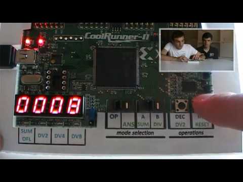
5. Introduction to the CoolRunner-II CPLD Starter Board
What is the CoolRunner-II CPLD Starter Board?
The CoolRunner-II CPLD starter board is an evaluation and development platform designed to help engineers and hobbyists get started with CoolRunner-II CPLDs. It typically features an XC2C64A CoolRunner-II CPLD and various peripherals for prototyping and testing designs.
Download and install the appropriate Xilinx design software (ISE WebPACK or Vivado)
Install any necessary USB drivers for the programming cable
Update your system’s environment variables if required
First Connection Setup
Connect the USB cable between your computer and the CoolRunner-II development board
Power on the board (if it has a separate power switch)
Verify that the board is recognized by your computer
Configuring the XC2C64A CoolRunner-II CPLD
Launch the Xilinx design software
Create a new project, selecting the XC2C64A as the target device
Write your VHDL or Verilog code
Synthesize and implement the design
Generate the programming file
Use the programming tool to configure the CPLD on the development board
7. First Project: Hello World with CoolRunner-II
Simple Project: Blinking LED
Let’s create a simple “Hello World” project that blinks an LED on the CoolRunner-II development board.
Writing a Basic VHDL Program
Here’s a simple VHDL code to blink an LED:
vhdl复制libraryIEEE;
use IEEE.STD_LOGIC_1164.ALL;
use IEEE.NUMERIC_STD.ALL;
entity blink_led is
Port ( clk : in STD_LOGIC;
led : out STD_LOGIC);
end blink_led;
architecture Behavioral of blink_led is
signal counter : unsigned(23 downto 0) := (others => '0');
begin
process(clk)
begin
if rising_edge(clk) then
counter <= counter + 1;
if counter(23) = '1' then
led <= '1';
else
led <= '0';
end if;
end if;
end process;
end Behavioral;
Synthesizing, Implementing, and Programming the Device
Create a new project in Xilinx ISE or Vivado
Add the VHDL file to your project
Set the XC2C64A as the target device
Run synthesis and implementation
Generate the programming file
Use the programmer tool to configure the CPLD
Troubleshooting Tips for Beginners
Double-check your pin assignments in the constraints file
Verify that the clock source is correctly configured
Use the software’s built-in simulation tools to test your design before programming
If the LED doesn’t blink, try adjusting the counter size or clock frequency
8. Expanding Your CoolRunner-II Projects
Using Onboard Switches and LEDs for Input/Output
Expand your projects by incorporating the onboard switches and LEDs:
Use switches as input signals
Control multiple LEDs for more complex output patterns
Implement debouncing for switch inputs
Creating State Machines
State machines are powerful tools for controlling system behavior:
Implement a simple traffic light controller
Create a sequence detector using switch inputs
Design a basic elevator controller
Interface Examples: UART, SPI, I2C Bridging
CoolRunner-II CPLDs excel at interfacing different protocols:
Implement a UART to SPI bridge
Create an I2C to parallel bus converter
Design a custom communication protocol using available I/O
Power Optimization Tricks for Mobile Designs
To maximize battery life in portable applications:
Utilize the CoolRunner-II’s power-down modes
Implement clock gating for unused modules
Use the lowest possible operating voltage for your design
9. Where to Buy CoolRunner-II CPLD Boards and Parts
Recommended Vendors and Distributors
Digikey
Mouser Electronics
Arrow Electronics
Avnet
Finding an XC2C64A CoolRunner-II CPLD Development Board Affordably
Check for educational discounts if you’re a student or academic institution
Look for bundle deals that include software and accessories
Consider purchasing refurbished or older model boards for cost savings
Tips for Checking Compatibility and Authenticity
Verify that the board supports the specific CoolRunner-II CPLD model you need
Check for official Xilinx branding and documentation
Ensure the board is compatible with your version of Xilinx design software
Conclusion
The Xilinx CoolRunner-II CPLD remains a popular choice for designers seeking a low-power, versatile programmable logic solution. Its unique combination of ultra-low power consumption, instant-on capability, and robust feature set makes it ideal for a wide range of applications, from portable electronics to industrial control systems.
By starting with simple projects and gradually exploring more advanced features, you can unlock the full potential of the CoolRunner-II CPLD. The CoolRunner II development board provides an excellent platform for learning and prototyping, allowing you to bring your digital designs to life quickly and efficiently.
As you continue your journey with CoolRunner-II CPLDs, remember to experiment, explore new applications, and leverage the wealth of resources available from Xilinx and the broader CPLD community. With its enduring relevance and capabilities, the CoolRunner-II CPLD is sure to remain a valuable tool in your digital design toolkit for years to come.
Frequently Asked Questions (FAQ)
Q1: Is CoolRunner-II still supported by Xilinx?
A: While newer Xilinx products have been introduced, CoolRunner-II CPLDs are still supported through the Xilinx ISE WebPACK software. However, they are not supported in the newer Vivado Design Suite.
Q2: What is the difference between CoolRunner-II and Spartan FPGA?
A: CoolRunner-II is a CPLD family optimized for low power and instant-on applications, while Spartan FPGAs offer higher logic density and more advanced features but typically consume more power and require configuration upon startup.
Q3: Can I use CoolRunner-II CPLDs in new designs?
A: Yes, CoolRunner-II CPLDs are still suitable for new designs, especially in applications requiring low power consumption and instant-on functionality. However, consider future availability and support when making long-term design decisions.
Q4: What programming languages can I use with CoolRunner-II CPLDs?
A: CoolRunner-II CPLDs can be programmed using hardware description languages (HDLs) such as VHDL and Verilog. The choice between these languages often depends on personal preference or project requirements.
Q5: How does the power consumption of CoolRunner-II compare to other CPLDs?
A: CoolRunner-II CPLDs are known for their ultra-low power consumption, often outperforming other CPLD families in this aspect. This makes them particularly suitable for battery-operated and portable devices.
In the ever-evolving world of digital electronics, Field-Programmable Gate Arrays (FPGAs) have become indispensable components for designers and engineers. Among the myriad of FPGA options available, the XC7A100T-1CSG324C stands out as a powerful and versatile choice. This comprehensive guide delves into the details of this Xilinx Artix-7 FPGA, exploring its datasheet, pinout configuration, key features, and pricing information. Whether you’re a seasoned engineer or a curious enthusiast, this article will provide valuable insights into the capabilities and applications of the XC7A100T-1CSG324C.
The XC7A100T-1CSG324C is part of the Xilinx Artix-7 FPGA family, known for its balance of low power consumption and high performance. Artix-7 FPGAs are designed to meet the needs of cost-sensitive applications while delivering impressive processing capabilities.
Decoding the Part Number
Let’s break down the part number to understand its specifications:
Understanding the pinout of the XC7A100T-1CSG324C is crucial for proper PCB design and integration. The 324-pin CSG package offers a compact form factor with ample I/O capabilities.
Key Pinout Sections
Power Supply Pins: Multiple VCC and GND pins for core, auxiliary, and I/O power.
Configuration Pins: Dedicated pins for device configuration and programming.
Clock Input Pins: Specialized pins for high-speed clock inputs.
User I/O Pins: General-purpose input/output pins, configurable for various standards.
Transceiver Pins: High-speed serial I/O pins for GTP transceivers.
JTAG Interface Pins: For boundary scan and device programming.
Pinout Considerations
Bank Organization: I/O pins are organized into banks, each supporting different voltage standards.
Differential Pairs: Certain pins can be configured as differential pairs for high-speed signaling.
Special Function Pins: Some pins have dual functionality, serving as both user I/O and special functions like configuration or clocking.
Key Features of the XC7A100T-1CSG324C
The XC7A100T-1CSG324C boasts a range of features that make it suitable for various applications. Let’s explore some of its standout capabilities:
1. Low Power Consumption
One of the hallmarks of the Artix-7 family is its energy efficiency. The XC7A100T-1CSG324C incorporates several power-saving features:
Intelligent Clock Gating: Automatically reduces dynamic power consumption by disabling unused clock networks.
Flexible Power Management: Allows designers to optimize power usage based on performance requirements.
Low-Power Gigabit Transceivers: GTP transceivers offer high-speed communication with minimal power overhead.
2. High-Performance DSP Capabilities
With 240 DSP slices, the XC7A100T-1CSG324C excels in digital signal processing applications:
Advanced DSP48E1 Slices: Support a wide range of symmetric and asymmetric filter structures.
High-Speed Arithmetic: Capable of performing up to 930 GMACs (Giga Multiply-Accumulate Operations per Second).
Flexible Precision: Supports various data widths, from 8-bit to 48-bit operations.
3. Versatile Memory Options
The XC7A100T-1CSG324C offers a variety of memory resources to suit different application needs:
Block RAM: 4.9 Mb of fast, on-chip memory configurable as single or dual-port RAM.
Distributed RAM: Up to 1,188 Kb of RAM implemented using LUTs for small, distributed memory structures.
Shift Register LUTs: Efficient implementation of shift registers and delay lines.
4. Advanced Clocking Technology
Precise clock management is crucial for high-performance designs. The XC7A100T-1CSG324C provides:
Mixed-Mode Clock Managers (MMCMs): 6 MMCMs for flexible clock synthesis and jitter reduction.
Phase-Locked Loops (PLLs): 6 PLLs for additional clock management options.
Low-Jitter Clock Networks: Ensures precise timing across the device.
5. High-Speed Serial Connectivity
The inclusion of GTP transceivers enables high-speed serial communication:
4 GTP Transceivers: Support data rates up to 6.6 Gb/s.
Integrated PCIe® Endpoint Block: Simplifies implementation of PCI Express interfaces.
Flexible Protocol Support: Compatible with a wide range of serial protocols, including SATA, DisplayPort, and JESD204B.
6. Robust I/O Capabilities
With up to 210 single-ended I/O pins, the XC7A100T-1CSG324C offers extensive connectivity options:
SelectIO™ Technology: Supports a wide range of I/O standards, including LVCMOS, LVDS, and SSTL.
High-Performance Memory Interfaces: Capable of interfacing with DDR3 SDRAM at speeds up to 1066 Mb/s.
Flexible I/O Banking: Allows mixing of different I/O standards within the same bank.
Applications of the XC7A100T-1CSG324C
The versatility of the XC7A100T-1CSG324C makes it suitable for a wide range of applications across various industries:
Industrial Automation: Used in motor control systems, robotics, and process control equipment.
Medical Devices: Enables high-performance image processing and data analysis in medical imaging systems.
Consumer Electronics: Powers advanced features in smart home devices and entertainment systems.
Telecommunications: Facilitates signal processing and protocol implementation in network equipment.
Automotive: Supports advanced driver assistance systems (ADAS) and in-vehicle infotainment.
Aerospace and Defense: Used in radar systems, secure communications, and electronic warfare applications.
Pricing and Availability
The pricing of the XC7A100T-1CSG324C can vary based on factors such as quantity, supplier, and market conditions. As of [current year], the typical price range for this FPGA is:
Single Unit: 80−80−120 USD
Volume Pricing (1000+ units): 60−60−90 USD per unit
It’s important to note that prices can fluctuate, and it’s best to consult with authorized distributors or Xilinx directly for the most up-to-date pricing information.
Availability Considerations
Lead Time: Typical lead times range from 8 to 16 weeks, depending on demand and production capacity.
Authorized Distributors: Purchase through authorized channels to ensure genuine products and proper support.
Lifecycle: As part of the Artix-7 family, the XC7A100T-1CSG324C has a long product lifecycle, ensuring availability for extended periods.
Design Tools and Resources
To fully leverage the capabilities of the XC7A100T-1CSG324C, Xilinx provides a comprehensive suite of design tools and resources:
1. Vivado Design Suite
Integrated Design Environment: Offers a complete toolset for RTL-to-bitstream design flow.
High-Level Synthesis: Enables C, C++, and SystemC designs to be directly implemented in the FPGA.
IP Integrator: Simplifies the process of integrating various IP cores into your design.
2. Vitis Unified Software Platform
AI Development: Tools for implementing machine learning algorithms on the FPGA.
Acceleration Libraries: Pre-optimized libraries for common functions to speed up development.
3. Documentation and Support
User Guides: Comprehensive documentation covering all aspects of the device and design process.
Application Notes: Detailed guides for implementing specific features and interfaces.
Reference Designs: Pre-built examples demonstrating common use cases and best practices.
Conclusion
The XC7A100T-1CSG324C FPGA represents a powerful and versatile solution for a wide range of applications. Its combination of low power consumption, high-performance DSP capabilities, and robust I/O options make it an excellent choice for designers seeking a balance of cost and functionality.
By understanding the datasheet specifications, pinout configuration, key features, and pricing considerations, engineers can make informed decisions about incorporating the XC7A100T-1CSG324C into their designs. Whether you’re developing industrial automation systems, medical devices, or cutting-edge consumer electronics, this Artix-7 FPGA provides the flexibility and performance needed to bring innovative ideas to life.
As FPGA technology continues to evolve, the XC7A100T-1CSG324C stands as a testament to the ongoing pursuit of higher performance, lower power consumption, and increased design flexibility in the world of programmable logic devices.
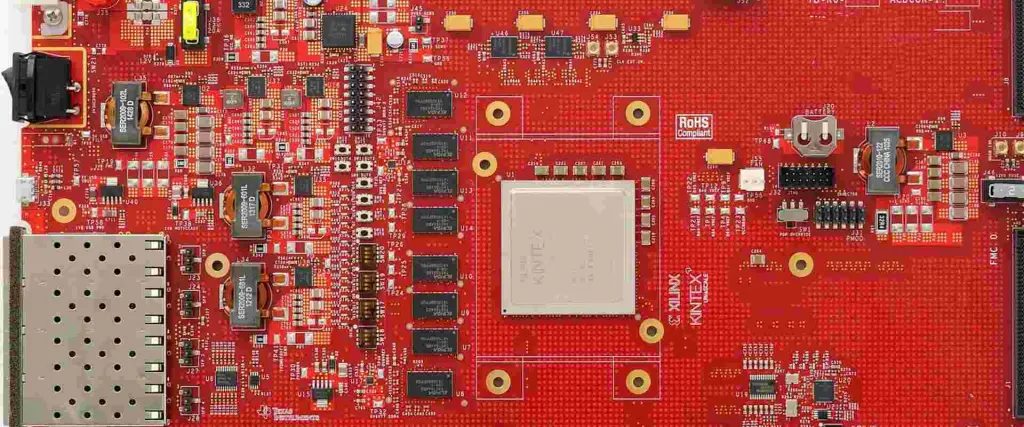
The XCKU060-1FFVA1517I is a high-performance Field-Programmable Gate Array (FPGA) from Xilinx’s Kintex UltraScale family. This powerful device offers an excellent balance of performance, power efficiency, and cost-effectiveness, making it ideal for a wide range of applications in telecommunications, data centers, medical imaging, and more. In this comprehensive guide, we’ll explore the key features, specifications, pinout details, and design considerations for the XCKU060-1FFVA1517I.
Overview of the Xilinx Kintex UltraScale FPGA Family
The UltraScale Architecture
The Xilinx Kintex UltraScale FPGA family, including the XCKU060-1FFVA1517I, is built on the advanced UltraScale architecture. This architecture offers significant improvements over previous generations, providing enhanced performance, reduced power consumption, and increased design flexibility.
The XCKU060-1FFVA1517I is a mid-range device within the Kintex UltraScale family, offering a balance of resources suitable for a variety of applications.
Key Specifications
Logic Cells: 725,550
CLB Flip-Flops: 663,360
CLB LUTs: 331,680
Maximum Distributed RAM (Mb): 10.9
Block RAM Blocks: 1,080
Total Block RAM (Mb): 38.9
UltraRAM Blocks: 0
DSP Slices: 2,760
CMTs: 12
Maximum HP I/O: 520
Maximum HD I/O: 96
System Monitor: 1
Package Information
The XCKU060-1FFVA1517I comes in an FFVA1517 package, which is a flip-chip fine-pitch ball grid array (BGA) package with 1,517 pins.
Datasheet Highlights
Power Management
The XCKU060-1FFVA1517I features advanced power management capabilities, including:
Multiple Power Domains: Allows for fine-grained control of power consumption
Power Gating: Ability to shut down unused portions of the chip
Intelligent Clock Gating: Reduces dynamic power consumption
Clock Management
Efficient clock management is crucial for high-performance designs. The XCKU060-1FFVA1517I offers:
Mixed-Mode Clock Managers (MMCMs): 12 MMCMs for flexible clock synthesis and manipulation
Phase-Locked Loops (PLLs): 24 PLLs for precise clock synchronization
Global Clock Buffers: 544 global clock buffers for distributing clock signals
I/O Capabilities
The device provides versatile I/O options to support various interfaces:
High-Performance (HP) I/O: Up to 520 user I/O pins
High-Density (HD) I/O: Up to 96 user I/O pins
GTH Transceivers: 48 GTH transceivers supporting up to 16.3 Gb/s
The FFVA1517 package used by the XCKU060-1FFVA1517I has a 40 x 40 ball grid array layout. The pins are arranged in a manner that optimizes signal integrity and minimizes crosstalk.
I/O Bank Organization
The I/O pins are organized into banks, each supporting different voltage standards:
HP I/O Banks: Support a wide range of single-ended and differential I/O standards
HD I/O Banks: Offer high-density connectivity for memory interfaces and other applications
GTH Transceiver Banks: Provide high-speed serial connectivity
Power Supply Pins
The XCKU060-1FFVA1517I requires multiple power supply voltages for different parts of the chip:
VCCINT: Core voltage supply
VCCAUX: Auxiliary voltage supply
VCCBRAM: Block RAM supply voltage
VCCIO: I/O bank supply voltage (varies depending on I/O standard)
Ground Pins
Proper grounding is essential for signal integrity and power distribution. The XCKU060-1FFVA1517I has numerous ground pins distributed across the package.
Design Guide
Design Flow Overview
Designing with the XCKU060-1FFVA1517I involves several key steps:
Requirements Analysis: Define the project requirements and constraints
Architecture Design: Create a high-level design of the system
RTL Development: Write the VHDL or Verilog code for the design
Synthesis: Convert the RTL code into a netlist of FPGA primitives
Implementation: Place and route the design on the FPGA fabric
Timing Analysis: Verify that the design meets timing requirements
Bitstream Generation: Create the configuration file for the FPGA
Tools and Software
Xilinx provides a comprehensive suite of tools for designing with the XCKU060-1FFVA1517I:
Vivado Design Suite: The primary integrated development environment (IDE) for UltraScale FPGAs
Vitis: Unified software platform for developing embedded software and accelerated applications
System Generator for DSP: High-level tool for DSP design on FPGAs
Best Practices for High-Performance Design
To achieve optimal performance with the XCKU060-1FFVA1517I, consider the following best practices:
Efficient Use of DSP Slices: Leverage the high-performance DSP slices for arithmetic operations
Memory Optimization: Use the appropriate mix of distributed RAM, block RAM, and UltraRAM
Clock Domain Management: Carefully plan and implement clock domains to minimize skew and maximize performance
Power Optimization: Utilize power gating and clock gating features to reduce power consumption
I/O Planning: Carefully plan I/O assignments to minimize signal crosstalk and maximize signal integrity
Debugging and Verification
Xilinx provides several features and tools to aid in debugging and verifying designs on the XCKU060-1FFVA1517I:
Integrated Logic Analyzer (ILA): On-chip debug tool for real-time signal monitoring
Virtual I/O (VIO): Allows for dynamic probing and control of internal signals
Vivado Simulator: Integrated simulator for functional and timing simulation
Hardware Manager: Tool for programming and interacting with the FPGA
Application Areas
The XCKU060-1FFVA1517I is suitable for a wide range of applications, including:
Telecommunications: 5G infrastructure, network processing, and packet processing
Data Centers: Network interface cards, storage controllers, and compute acceleration
Medical Imaging: Image processing and analysis for MRI, CT, and ultrasound systems
Industrial Automation: Motion control, robotics, and machine vision
Aerospace and Defense: Radar systems, electronic warfare, and secure communications
Performance Benchmarks
DSP Performance
The XCKU060-1FFVA1517I excels in DSP-intensive applications:
Symmetric FIR Filter: Up to 2,760 GMACs (Giga Multiply-Accumulate operations per second)
FFT Performance: Capable of processing large FFTs with low latency
Memory Bandwidth
With its extensive memory resources, the XCKU060-1FFVA1517I offers impressive memory bandwidth:
Block RAM: Up to 4,503 Gb/s peak bandwidth
Distributed RAM: Additional low-latency memory option for small data structures
Transceiver Performance
The GTH transceivers in the XCKU060-1FFVA1517I support high-speed serial communication:
Maximum Data Rate: Up to 16.3 Gb/s per transceiver
Aggregate Bandwidth: Up to 782.4 Gb/s (48 transceivers)
Comparison with Other Kintex UltraScale Devices
XCKU060-1FFVA1517I vs. XCKU040
Logic Cells: XCKU060 has 725,550 vs. XCKU040’s 530,250
DSP Slices: XCKU060 has 2,760 vs. XCKU040’s 1,920
Block RAM: XCKU060 has 38.9 Mb vs. XCKU040’s 21.1 Mb
XCKU060-1FFVA1517I vs. XCKU095
Logic Cells: XCKU060 has 725,550 vs. XCKU095’s 1,176,000
DSP Slices: XCKU060 has 2,760 vs. XCKU095’s 4,100
Block RAM: XCKU060 has 38.9 Mb vs. XCKU095’s 54.8 Mb
Conclusion
The XCKU060-1FFVA1517I Xilinx Kintex UltraScale FPGA offers a powerful and flexible platform for a wide range of high-performance applications. With its balanced mix of logic, memory, and DSP resources, coupled with high-speed transceivers and advanced power management features, this device is well-suited for demanding tasks in telecommunications, data centers, medical imaging, and more.
By leveraging the comprehensive tools provided by Xilinx and following best design practices, engineers can fully utilize the capabilities of the XCKU060-1FFVA1517I to create innovative and efficient solutions. As the demand for high-performance, low-power computing continues to grow, the XCKU060-1FFVA1517I stands as a compelling choice for designers looking to push the boundaries of what’s possible with FPGA technology.