In the realm of electronic design, Printed Circuit Boards (PCBs) serve as the foundation for countless devices and systems. As technology advances and circuit densities increase, the challenges associated with electromagnetic interference (EMI) and proper grounding become more pronounced. This article delves into the critical aspects of anti-interference techniques and grounding strategies for PCBs, providing a comprehensive analysis of best practices and innovative solutions.
Understanding Electromagnetic Interference in PCBs
Types of EMI
Electromagnetic interference in PCBs can be categorized into two main types:
- Conducted EMI: Interference that propagates through conductive paths.
- Radiated EMI: Interference that propagates through space as electromagnetic waves.
Sources of EMI
Common sources of EMI in PCB designs include:
- High-frequency digital circuits
- Switching power supplies
- Clock signals
- High-speed data lines
- External environmental factors
Effects of EMI on PCB Performance
EMI can lead to various issues in PCB operation:
- Signal integrity degradation
- Increased noise in analog circuits
- False triggering of digital circuits
- Reduced overall system reliability
Anti-Interference Strategies for PCBs

1. PCB Layout Optimization
Component Placement
Proper component placement is crucial for minimizing EMI:
- Separate digital and analog sections
- Group similar components together
- Place high-frequency components close to their associated circuitry
Trace Routing
Optimizing trace routing can significantly reduce EMI:
- Use short, direct traces for critical signals
- Avoid 90-degree bends in high-speed traces
- Implement differential pair routing for high-speed signals
Layer Stack-up Design
An effective layer stack-up can provide inherent EMI shielding:
LayerTypePurposeTopSignalHigh-speed signals2GroundEMI shielding3PowerPower distribution4GroundEMI shielding5SignalLow-speed signalsBottomGroundEMI shielding
2. Shielding Techniques
Board-Level Shielding
- Faraday cages: Enclosing sensitive components in metal shields
- Guard traces: Implementing grounded traces around sensitive signals
System-Level Shielding
- Metallic enclosures: Using conductive cases to contain EMI
- Gaskets and conductive coatings: Ensuring continuity of shielding at seams and interfaces
3. Filtering and Decoupling
Power Supply Filtering
Implementing effective power supply filtering reduces conducted EMI:
| Filter Type | Typical Application | Effectiveness |
| LC Filter | Low-frequency noise | High |
| Ferrite Bead | High-frequency noise | Medium to High |
| Pi Filter | Broadband noise | Very High |
Decoupling Capacitors
Proper use of decoupling capacitors is crucial for noise suppression:
- Place close to power pins of ICs
- Use a combination of capacitor values for broadband effectiveness
- Consider low-ESR capacitors for high-frequency applications
4. Signal Integrity Techniques
Impedance Matching
Proper impedance matching reduces signal reflections and associated EMI:
- Use controlled impedance traces for high-speed signals
- Implement termination resistors at the end of transmission lines
Differential Signaling
Utilizing differential signaling can significantly reduce EMI:
- Provides inherent noise cancellation
- Reduces common-mode noise
Grounding Strategies for PCBs
1. Ground Plane Design
Solid Ground Planes
Implementing solid ground planes offers several benefits:
- Provides low-impedance return paths for signals
- Reduces ground bounce and noise
- Acts as a shield against EMI
Split Ground Planes
In mixed-signal designs, consider split ground planes:
- Separate analog and digital grounds
- Connect at a single point to prevent ground loops
2. Star Grounding
Implementing a star grounding scheme can be effective in certain designs:
- All ground connections return to a single point
- Minimizes common impedance coupling
3. Ground Islands
For sensitive analog circuits, consider using ground islands:
- Isolate sensitive circuits from noisy digital grounds
- Connect to the main ground at a single point
4. Grounding for Multi-Layer PCBs
Effective grounding strategies for multi-layer PCBs:
| Layer Configuration | Grounding Strategy |
| 2-layer | Dedicate one layer to ground |
| 4-layer | Use inner layers for power and ground |
| 6+ layer | Alternate signal and ground/power layers |
5. Grounding for High-Speed Circuits
Special considerations for high-speed circuit grounding:
- Use multiple vias for ground connections to reduce inductance
- Implement ground planes on adjacent layers to high-speed signal layers
- Consider stitching capacitors between split ground planes
Advanced Anti-Interference and Grounding Techniques
1. Electromagnetic Band Gap (EBG) Structures
EBG structures can provide effective EMI suppression:
- Create frequency band gaps that prevent EMI propagation
- Can be implemented in PCB layout for targeted frequency suppression
2. Active EMI Cancellation
Implementing active EMI cancellation techniques:
- Use sensors to detect EMI
- Generate cancellation signals to neutralize detected EMI
3. Spread Spectrum Clocking
Utilizing spread spectrum clocking can reduce peak EMI emissions:
- Spreads the energy of clock signals over a wider frequency range
- Typically results in a 5-10 dB reduction in peak emissions
4. Embedded Capacitance
Implementing embedded capacitance in PCB design:
- Use thin dielectric layers between power and ground planes
- Provides distributed capacitance, reducing the need for discrete decoupling capacitors
Practical Implementation and Testing
1. EMI Pre-Compliance Testing
Conducting pre-compliance testing during the design phase:
- Use near-field probes to identify EMI hotspots
- Perform radiated and conducted emissions tests
2. Iterative Design Process
Implement an iterative design process for EMI mitigation:
- Design initial PCB layout
- Perform EMI testing and analysis
- Identify problem areas and implement solutions
- Retest and refine design
3. Simulation Tools
Utilize EMI simulation tools for predictive analysis:
- 3D electromagnetic field solvers
- Circuit-level EMI simulators
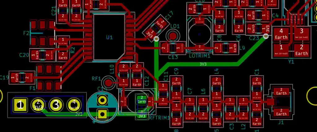
Case Study: EMI Reduction in a High-Speed Digital PCB
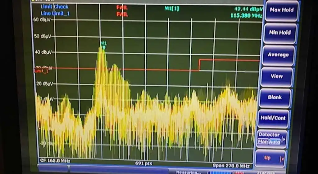
Consider a case study of a high-speed digital PCB experiencing EMI issues:
Initial Design Characteristics
- 6-layer PCB with mixed analog and digital circuits
- Clock frequency: 200 MHz
- Failing EMI tests at 600 MHz and 1.2 GHz
Implemented Solutions and Results
| Solution | Implementation | EMI Reduction |
| Optimized stackup | Added ground layers adjacent to signal layers | -5 dB |
| Improved decoupling | Added local and bulk decoupling capacitors | -8 dB |
| Shielding | Implemented board-level shielding for sensitive areas | -12 dB |
| Spread spectrum clocking | Applied 0.5% down-spreading to main clock | -4 dB |
| Trace routing optimization | Rerouted critical signals with controlled impedance | -3 dB |
Total EMI reduction: Approximately -32 dB
This case study demonstrates the cumulative effect of implementing multiple EMI reduction techniques, resulting in significant improvement in EMI performance.
Conclusion
Effective anti-interference and grounding strategies are crucial for ensuring the reliable operation of PCBs in increasingly complex and noisy electromagnetic environments. By implementing a combination of layout optimization, shielding, filtering, and advanced grounding techniques, designers can significantly reduce EMI issues and improve overall system performance.
The strategies outlined in this article provide a comprehensive toolkit for addressing EMI challenges in PCB design. From fundamental techniques like proper component placement and trace routing to advanced methods such as EBG structures and active EMI cancellation, designers have a wide array of options to tackle interference problems.
As electronic systems continue to evolve with higher speeds and greater integration, the importance of effective EMI management and grounding will only grow. Staying informed about the latest anti-interference techniques and grounding strategies will be essential for engineers looking to create robust and reliable PCB designs in the future.
FAQ (Frequently Asked Questions)
Q1: How does the choice of PCB material affect EMI performance?
A1: The choice of PCB material can significantly impact EMI performance. Materials with lower dielectric constants (Dk) and loss tangents generally offer better EMI performance. For example, high-frequency PCB materials like Rogers RO4350B or Taconic RF-35 typically provide better EMI characteristics compared to standard FR-4. These materials reduce signal losses and minimize unwanted coupling between traces. However, they are often more expensive and may require special manufacturing processes. The decision on PCB material should balance EMI performance requirements with cost and manufacturability considerations.
Q2: What are the key differences in grounding strategies for analog and digital circuits?
A2: Grounding strategies for analog and digital circuits often differ due to their distinct noise sensitivities and current flow characteristics:
- Analog circuits:
- Prefer star grounding or single-point grounding to minimize ground loops
- May use separate analog ground planes isolated from digital noise
- Require careful attention to return current paths
- Digital circuits:
- Often use multi-point grounding with solid ground planes
- Can tolerate and benefit from multiple ground connections for reduced impedance
- Typically generate more high-frequency noise that needs containment
In mixed-signal designs, a common approach is to use separate analog and digital ground planes connected at a single point, often near the power supply or A/D converter.
Q3: How effective are ferrite beads in EMI suppression, and when should they be used?
A3: Ferrite beads can be highly effective for EMI suppression, particularly for high-frequency noise. They work by presenting a high impedance to high-frequency signals while allowing DC and low-frequency signals to pass with minimal attenuation. The effectiveness of ferrite beads depends on several factors:
| Frequency Range | Typical Attenuation |
| < 10 MHz | Low |
| 10 MHz – 1 GHz | High |
| > 1 GHz | Moderate to Low |
Ferrite beads are most commonly used:
- In power supply lines to filter high-frequency noise
- At board interfaces to prevent external noise from entering the PCB
- In clock or high-speed signal lines to reduce radiated emissions
They should be used cautiously in high-current paths, as they can saturate and lose effectiveness. For optimal performance, ferrite beads should be selected based on the specific frequency range of concern and the current requirements of the circuit.
Q4: What are the pros and cons of using a ground pour versus a solid ground plane?
A4: Ground pours and solid ground planes each have their advantages and disadvantages:
Ground Pour: Pros:
- Flexibility in routing on the same layer
- Can provide some EMI shielding
- Useful for thermal management in some designs
Cons:
- Higher impedance than solid planes, especially at high frequencies
- Can create isolated ground islands if not properly connected
- May introduce unpredictable return current paths
Solid Ground Plane: Pros:
- Lowest impedance return path for signals
- Provides excellent EMI shielding
- Simplifies impedance control for high-speed signals
Cons:
- Reduces routing flexibility on the ground layer
- May require additional layers in complex designs
- Can be more expensive due to increased copper usage
In general, solid ground planes are preferred for high-speed and sensitive analog designs due to their superior EMI performance and signal integrity benefits. Ground pours can be useful in simpler, low-speed designs or in areas where routing flexibility is crucial.
Q5: How can one effectively address EMI issues in flexible or rigid-flex PCBs?
A5: Addressing EMI in flexible or rigid-flex PCBs presents unique challenges due to their dynamic nature and often limited layer count. Here are some effective strategies:
- Use shielding layers: Incorporate flexible shielding materials or conductive films to provide EMI protection in flex areas.
- Optimize layer stackup: When possible, sandwich signal layers between ground layers to provide shielding.
- Careful routing: Avoid running high-speed or sensitive signals through flex areas if possible. When necessary, use differential pairs and control impedance carefully.
- Grounding considerations: Ensure proper grounding across the entire assembly, paying special attention to transitions between rigid and flex sections.
- Component placement: Place noise-sensitive components on rigid sections when possible.
- Use of ferrite beads: Implement ferrite beads at the transition between rigid and flex sections to suppress high-frequency noise.
- EMI-absorbing materials: Consider using EMI-absorbing materials in critical areas of the flex circuit.
- Minimize flex length: Keep flexible sections as short as possible to reduce their potential for acting as antennas.
- Simulation and testing: Utilize 3D EM simulation tools to model the flexible sections and perform thorough EMI testing, including tests with the PCB in various flex positions.
By implementing these strategies and carefully considering the unique aspects of flexible circuits, designers can effectively manage EMI issues in flexible and rigid-flex PCB designs.