Linear voltage regulators form the backbone of countless electronic systems, providing stable and reliable power conversion across a wide range of applications. From simple battery-powered devices to sophisticated industrial equipment, these regulators ensure that sensitive electronic components receive consistent voltage levels regardless of input variations or changing load conditions. This comprehensive analysis explores the fundamental operating principles of linear regulators, examines the key differences between traditional three-terminal regulators and low dropout (LDO) variants, and investigates the latest technological advances that are reshaping power management solutions.

Fundamental Architecture and Operating Principles
Linear regulators operate on two primary architectural configurations: series regulators and shunt regulators. While both serve the same fundamental purpose of voltage stabilization, series regulators—being far more common in practical applications—will be the focus of our discussion. These devices function as sophisticated closed-loop feedback systems that continuously monitor output conditions and dynamically adjust their internal resistance to maintain voltage stability.
The essence of linear regulation lies in its ability to act as a variable resistor that automatically adjusts its impedance in response to changing conditions. This dynamic adjustment mechanism enables the regulator to compensate for both input voltage fluctuations and load current variations, ensuring consistent output voltage delivery under diverse operating scenarios.
Dynamic Regulation During Input Voltage Variations
When examining the behavior of linear regulators under varying input conditions, the feedback control mechanism demonstrates remarkable sophistication. Consider a scenario where the input voltage experiences an increase—perhaps due to power grid fluctuations, switching noise from nearby equipment, or variations in the primary power supply. In an unregulated system, this input voltage increase would directly translate to a proportional rise in output voltage, potentially damaging sensitive downstream components.
However, in a properly designed linear regulator, the error amplifier continuously compares the actual output voltage against a stable reference voltage. When the input voltage increases, the initial tendency for the output voltage to rise is immediately detected by this error amplifier. In response, the control circuitry increases the impedance of the series pass element—effectively the variable resistor in our conceptual model.
This increased impedance serves a dual purpose: it dissipates the excess voltage differential as heat while simultaneously reducing the voltage transfer from input to output. The result is a form of “peak-clipping stabilization” where voltage spikes are absorbed by the regulator itself, maintaining a constant output voltage despite input variations. This process occurs continuously and rapidly, typically responding to input changes within microseconds.
The effectiveness of this regulation mechanism depends heavily on the design parameters of the error amplifier, including its gain bandwidth product, slew rate, and stability margins. Higher performance regulators incorporate sophisticated compensation networks and multi-stage amplification to achieve superior transient response and steady-state accuracy.
Load Current Variation Compensation
Equally important is the regulator’s ability to maintain voltage stability under changing load conditions. Modern electronic systems frequently exhibit dynamic power consumption patterns—processors that switch between idle and full-load states, communication modules that transmit in bursts, or motor drives that experience varying mechanical loads.
When load current decreases, the immediate effect is a reduction in the voltage drop across the series pass element, causing the output voltage to temporarily rise above its target value. The error amplifier detects this deviation and responds by increasing the impedance of the series pass element. This compensatory action maintains the proper voltage drop even with reduced current flow, effectively preventing output voltage drift.
Conversely, when load current increases, the initial voltage drop across the series pass element rises, temporarily reducing output voltage. The error amplifier responds by decreasing the series impedance, allowing more current to flow while maintaining the desired voltage differential. This dynamic impedance adjustment ensures stable output voltage across the entire specified load current range.
The speed and accuracy of this load regulation depend on several factors, including the loop gain of the feedback system, the output capacitance, and the equivalent series resistance (ESR) of the output capacitor. Proper selection of these components is crucial for achieving optimal transient response and minimizing output voltage ripple.
Three-Terminal Regulators: Traditional Approach and Limitations
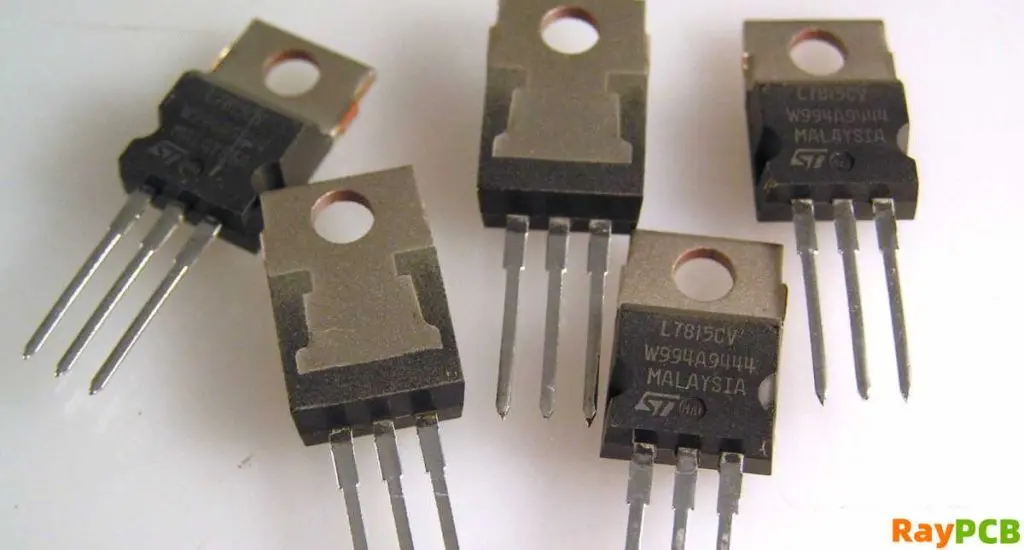
Traditional three-terminal regulators, exemplified by the ubiquitous 78xx series and similar devices, represent the foundational technology in linear voltage regulation. These regulators typically employ NPN bipolar junction transistors or N-channel MOSFETs as their series pass elements, positioned between the input and output terminals.
The fundamental limitation of three-terminal regulators lies in their relatively high dropout voltage requirements. For NPN-based designs, the minimum input-output voltage differential must satisfy the relationship: VIN – VOUT > RIN × IIN + 2 × VBE. This requirement stems from the need to maintain proper bias conditions for both the series pass transistor and the internal reference circuitry.
In practical terms, consider a typical scenario where RIN equals 1kΩ, input current (IIN) is 1mA, and the base-emitter voltage (VBE) is 0.7V. For a regulator designed to provide 5V output, the minimum input voltage requirement becomes 7.4V. This represents a dropout voltage of 2.4V—a significant overhead that translates directly to power dissipation and reduced efficiency.
MOSFET-based three-terminal regulators offer modest improvement, with the dropout voltage determined by VIN – VOUT > RIN × IIN + VGS. Using similar component values but with VGS = 1V, the minimum input voltage becomes 7V, representing a 0.4V improvement over the bipolar design.
While these dropout voltage requirements may seem manageable in high-voltage applications, they become increasingly problematic as system voltages decrease. In battery-powered applications, where maximizing operational time is critical, these relatively high dropout voltages represent significant inefficiency and reduced battery utilization.
LDO Regulators: Advancing the Technology
Low Dropout (LDO) regulators address the fundamental limitations of three-terminal regulators through innovative circuit topologies and component selection. The key breakthrough lies in their use of PNP bipolar transistors or P-channel MOSFETs as series pass elements, fundamentally altering the dropout voltage characteristics.
In PNP-based LDO designs, the minimum dropout voltage is determined by the collector-emitter saturation voltage (VCE(sat)), typically ranging from 0.1V to 0.3V depending on the specific transistor characteristics and operating current. This represents a dramatic improvement over traditional designs, enabling effective regulation even when input and output voltages are closely matched.
P-channel MOSFET implementations offer even better performance, with dropout voltages determined by the drain-source resistance (RDS(ON)) multiplied by the drain current (VDS = RDS(ON) × ID). Modern P-channel MOSFETs can achieve RDS(ON) values below 100 milliohms, resulting in dropout voltages well under 100mV at moderate current levels.
The practical implications of these improvements are substantial. An LDO regulator can maintain 3.3V output with input voltages as low as 3.5V, compared to traditional regulators that might require 5V or higher. This capability is particularly valuable in battery-powered applications, where it enables utilization of a greater portion of the battery’s capacity.
Beyond the primary advantage of reduced dropout voltage, LDO regulators typically offer superior line and load regulation, lower output noise, and better transient response compared to their three-terminal counterparts. These improvements stem from more sophisticated internal circuitry, including enhanced error amplifiers, improved reference voltage sources, and optimized compensation networks.
Next-Generation LDO Technology: N-Channel MOSFET Innovation
The evolution of LDO technology continues with the development of advanced regulators that push dropout voltage performance even further. These next-generation devices achieve their superior performance through the innovative use of N-channel MOSFETs, which inherently offer lower on-resistance compared to P-channel devices of equivalent size and cost.
The physics behind this advantage lies in the fundamental differences between electron and hole mobility in silicon. N-channel MOSFETs, which rely on electron conduction, can achieve significantly lower RDS(ON) values than P-channel devices, which depend on hole conduction. This translates directly to lower dropout voltages and reduced power dissipation.
However, implementing N-channel MOSFETs in LDO applications presents significant design challenges. Unlike P-channel devices that can be directly connected between input and output, N-channel MOSFETs require gate voltages higher than the input voltage to achieve proper conduction. This necessitates sophisticated control circuitry, including charge pump circuits or bootstrap techniques to generate the required gate drive voltage.
Modern implementations address these challenges through integrated solutions that combine the N-channel MOSFET with dedicated driver circuitry and auxiliary power supplies. These designs typically include separate bias voltage sources, ensuring stable operation across the full input voltage range while maintaining the low dropout advantages.
Advanced LDO Features and Performance Characteristics
Contemporary LDO regulators incorporate numerous advanced features that extend their applicability and improve system-level performance. Current limiting protection prevents device damage during short-circuit conditions, while thermal shutdown circuitry provides additional safety margins during high-temperature operation.
Many modern LDOs include enable/disable functionality, allowing system-level power management and sequencing control. This feature is particularly valuable in complex systems where different circuit blocks must be powered up or down in specific sequences to prevent latch-up or other undesirable conditions.
Noise performance represents another critical advancement area. High-performance LDOs achieve output noise levels below 50µVRMS across the audio frequency spectrum, making them suitable for sensitive analog applications including precision measurement systems and high-resolution data acquisition circuits.
Practical Applications and Selection Considerations
The choice between traditional three-terminal regulators, standard LDOs, and advanced N-channel LDOs depends on specific application requirements. Three-terminal regulators remain cost-effective solutions for high-voltage applications where dropout voltage is not critical, such as transforming 12V supplies to 5V logic levels.
Standard LDO regulators excel in battery-powered applications, precision analog circuits, and any scenario where input-output voltage differentials are small. Their superior regulation performance and low noise characteristics make them ideal for powering sensitive analog front-ends, precision references, and low-noise amplifiers.
Advanced N-channel LDO regulators find applications in the most demanding scenarios, such as point-of-load regulation in high-performance processors, battery-powered wireless communication systems, and portable medical devices where maximum efficiency and minimum dropout voltage are paramount.
Conclusion
The evolution from traditional three-terminal regulators to advanced LDO technology represents a significant advancement in power management capabilities. Through innovative circuit topologies, advanced semiconductor processes, and sophisticated control techniques, modern LDO regulators deliver unprecedented performance levels that enable new categories of electronic systems.
As electronic devices continue to demand lower operating voltages, higher efficiency, and improved performance, LDO regulator technology will undoubtedly continue evolving. Future developments may include adaptive dropout voltage control, integrated power monitoring, and even greater integration with digital control systems, further expanding the role of linear regulators in modern electronic design.
Understanding these technologies and their trade-offs enables engineers to make informed decisions when selecting power management solutions, ultimately leading to more efficient, reliable, and capable electronic systems.