Printed Circuit Board (PCB) chip package soldering is a critical process in electronic manufacturing that demands precision, technical expertise, and a thorough understanding of various soldering techniques. This comprehensive guide will explore the intricate world of chip package soldering, providing detailed insights into methods, processes, and best practices.
Understanding Chip Packages
Types of Chip Packages
| Package Type | Characteristics | Common Applications |
| DIP (Dual In-line Package) | Through-hole mounting | Older electronics, prototyping |
| QFP (Quad Flat Package) | Surface mount | Microcontrollers, processors |
| BGA (Ball Grid Array) | High-density interconnection | Advanced computing, telecommunications |
| SOIC (Small Outline Integrated Circuit) | Compact surface mount | General electronic devices |
Package Selection Considerations
- Electrical Requirements
- Pin count
- Signal integrity
- Power consumption
- Mechanical Constraints
- Board space
- Thermal management
- Mechanical stress tolerance
Soldering Methods
Surface Mount Technology (SMT)
Reflow Soldering Process
| Stage | Temperature Range | Primary Purpose |
| Preheat | 100-150°C | Remove moisture |
| Soak | 150-180°C | Activate flux |
| Reflow | 217-250°C | Melt solder |
| Cooling | 50-100°C | Solidify connection |
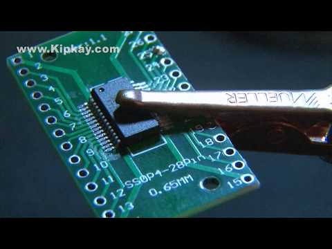
Through-Hole Soldering
Manual Soldering Techniques
- Hand Soldering Process
- Use temperature-controlled soldering iron
- Select appropriate tip size
- Apply minimal heat duration
- Specialized Techniques
- Wave soldering for multiple components
- Selective soldering for complex boards
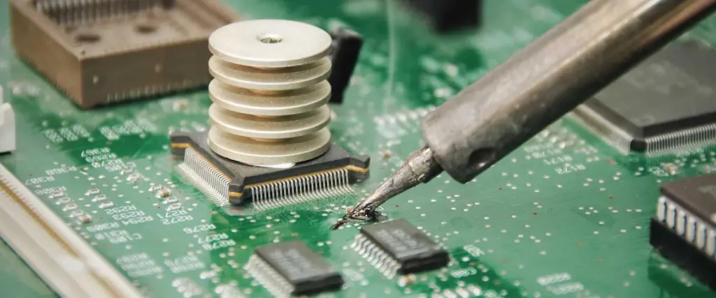
Advanced Soldering Technologies
Specialized Soldering Methods
- Vapor Phase Soldering
- Uniform heating
- Minimized thermal stress
- Ideal for complex packages
- Laser Soldering
- Precise heat application
- Minimal thermal impact
- Suitable for sensitive components
Preparation and Pre-Soldering Considerations
Workspace Setup
| Essential Element | Recommended Specification |
| Workspace Temperature | 20-25°C |
| Humidity Control | 40-60% relative humidity |
| Lighting | Bright, even illumination |
| Anti-Static Protection | Grounded workspace |
Component Handling Protocols
- Electrostatic Discharge (ESD) Protection
- Use grounded wrist straps
- Implement static-free environments
- Handle components with care
- Component Storage
- Controlled temperature
- Moisture-barrier packaging
- Proper labeling and tracking
Soldering Process Flow

Comprehensive Soldering Workflow
- Pre-Soldering Preparation
- Inspect PCB and components
- Clean surfaces
- Apply flux if necessary
- Alignment and Placement
- Precise component positioning
- Verify orientation
- Minimal mechanical stress
- Soldering Execution
- Control temperature
- Minimize contact time
- Ensure complete solder coverage
- Post-Soldering Inspection
- Visual examination
- Electrical testing
- Thermal imaging (optional)
Defect Detection and Prevention
Common Soldering Defects
| Defect Type | Characteristics | Prevention Strategy |
| Solder Bridging | Unintended connections | Precise paste application |
| Cold Joints | Weak electrical connection | Proper temperature control |
| Tombstoning | Component lifting | Balanced thermal profile |
| Voiding | Internal solder gaps | Optimize reflow parameters |
Inspection Techniques
- Visual Inspection
- Magnification
- Lighting conditions
- Standardized evaluation criteria
- Advanced Testing
Thermal Management
Heat-Related Considerations
- Thermal Profiling
- Create precise temperature curve
- Account for component sensitivity
- Minimize thermal stress
- Cooling Strategies
- Controlled cooling rates
- Minimize thermal shock
- Implement heat sinks if required
Specialized Techniques for Complex Packages
Challenging Package Types
- BGA Soldering Challenges
- Invisible connections
- Precise alignment
- X-ray verification techniques
- Miniaturization Considerations
- Micro-soldering techniques
- Advanced optical alignment
- Precision equipment
Emerging Soldering Technologies
Future Trends
- Environmentally Friendly Processes
- Lead-free soldering
- Reduced chemical usage
- Sustainable manufacturing
- Automation and Precision
- Machine learning integration
- Robotic soldering systems
- Advanced process control
Frequently Asked Questions (FAQ)
Q1: What is the most critical factor in successful chip package soldering?
A: Precise temperature control and proper flux application are crucial. Consistent, controlled heat and clean surfaces ensure reliable solder joints.
Q2: How do I choose between different soldering methods?
A: Consider package type, component sensitivity, production volume, and available equipment. Each method has specific advantages for different scenarios.
Q3: What are the main challenges with BGA package soldering?
A: BGA packages have hidden connections, requiring advanced alignment techniques, X-ray inspection, and precise temperature profiling.
Q4: How can I minimize soldering defects?
A: Implement strict process controls, use high-quality materials, maintain clean work environments, and invest in proper training and equipment.
Q5: Are lead-free soldering techniques really necessary?
A: Yes, lead-free soldering is increasingly important due to environmental regulations and health considerations. Modern techniques have significantly improved reliability.
Conclusion
PCB chip package soldering represents a complex intersection of technical skill, scientific precision, and technological innovation. Mastering these techniques requires continuous learning, attention to detail, and a commitment to quality.
As electronic devices become increasingly sophisticated, soldering techniques will continue to evolve, demanding adaptability, expertise, and a deep understanding of emerging technologies.
