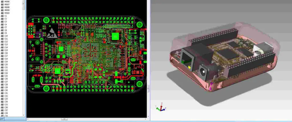
Autodesk EAGLE is a powerful PCB design software that includes essential features for ensuring design quality through Design Rule Check (DRC) and manufacturing preparation via Gerber file generation. This comprehensive guide explores both aspects in detail, providing crucial information for PCB designers and engineers.
Understanding Design Rule Check (DRC)
DRC Fundamentals
| DRC Aspect | Description | Importance |
| Clearance Rules | Minimum spacing requirements | Prevents shorts |
| Width Rules | Trace width specifications | Ensures current capacity |
| Drill Rules | Hole size and spacing | Manufacturing feasibility |
| Mask Rules | Solder mask parameters | Assembly quality |
Types of Design Rules
Electrical Rules
| Rule Type | Parameters | Common Values |
| Clearance | Min spacing between elements | 6-10 mil |
| Width | Min/max trace width | 8-12 mil |
| Drill Size | Min/max hole diameter | 0.3-0.4 mm |
| Annular Ring | Min copper around holes | 0.15-0.25 mm |
Manufacturing Rules
| Category | Parameters | Purpose |
| Layer Setup | Stack definition | Material specification |
| Mask Clearance | Solder mask openings | Component soldering |
| Minimum Feature | Smallest allowed feature | Manufacturability |
| Board Edge | Edge clearances | Board integrity |
Setting Up DRC in Eagle
Basic Setup Process
- Access Configuration
- Open DRC dialog
- Select rule categories
- Input parameters
- Save configuration
- Custom Rules Creation
- Define specific requirements
- Set layer-specific rules
- Configure special areas
- Establish exceptions
Running DRC Checks
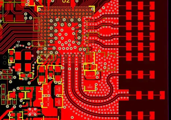
Check Categories
| Category | Elements Checked | Common Issues |
| Clearance | Component spacing | Overlapping traces |
| Connectivity | Signal continuity | Unconnected nets |
| Layer Usage | Layer assignments | Incorrect routing |
| Size Limits | Feature dimensions | Undersized elements |
Error Resolution
Common Errors
| Error Type | Possible Cause | Solution |
| Clearance Violation | Too close spacing | Adjust component placement |
| Width Error | Incorrect trace width | Modify trace properties |
| Drill Error | Invalid hole size | Update drill parameters |
| Mask Error | Incorrect mask setup | Adjust mask settings |
Gerber File Generation
Gerber File Basics
| File Type | Extension | Purpose |
| Top Copper | .GTL | Component side copper |
| Bottom Copper | .GBL | Solder side copper |
| Top Mask | .GTS | Component side mask |
| Bottom Mask | .GBS | Solder side mask |
| Silkscreen | .GTO/.GBO | Component marking |
| Drill File | .TXT | Hole locations |
Layer Configuration
Essential Layers
| Layer Name | Number | Content |
| Top Layer | 1 | Components and traces |
| Bottom Layer | 16 | Bottom side traces |
| Pads | 17 | Through-hole pads |
| Vias | 18 | Through-board connections |
| Dimension | 20 | Board outline |
Export Settings
| Parameter | Recommended Value | Purpose |
| Format | RS-274X | Industry standard |
| Units | Inches | Manufacturing preference |
| Resolution | 2:04 | Coordinate precision |
| Optimize | Yes | File size reduction |
Advanced DRC Configuration

Custom Rule Creation
- Specialized Rules
- High-speed signals
- Power distribution
- RF considerations
- Flex PCB requirements
- Rule Priority
- Global rules
- Net class rules
- Component rules
- Area rules
DRC Script Implementation
| Script Element | Function | Application |
| Rule Definition | Parameter setup | Basic rules |
| Conditional Rules | Specific cases | Special requirements |
| Error Handling | Issue management | Problem resolution |
| Documentation | Rule documentation | Reference material |
Gerber File Verification
Pre-Manufacturing Checks
Visual Verification
| Check Type | Elements to Verify | Tools Used |
| Layer Alignment | Registration marks | Gerber viewer |
| Feature Size | Minimum dimensions | Measurement tools |
| Text Readability | Silkscreen quality | Preview mode |
| Hole Position | Drill file accuracy | Overlay view |
Manufacturing Preparation
- File Organization
- Logical naming
- Layer grouping
- Version control
- Documentation
- Manufacturing Notes
- Board specifications
- Special requirements
- Material details
- Finish options
Best Practices
DRC Implementation
| Practice | Description | Benefit |
| Regular Checks | Frequent DRC runs | Early error detection |
| Custom Rules | Project-specific setup | Design optimization |
| Documentation | Rule documentation | Knowledge transfer |
| Version Control | Rule set management | Consistency |
Gerber Generation
Quality Assurance Steps
- Pre-Generation
- Design verification
- Layer confirmation
- Rule compliance
- Component check
- Post-Generation
- File completeness
- Layer accuracy
- Dimension verification
- Manufacturing review
Advanced Features
Automation Capabilities
| Feature | Function | Application |
| Batch DRC | Multiple checks | Large designs |
| Custom Scripts | Automated tasks | Repetitive processes |
| Report Generation | Documentation | Quality assurance |
| Integration | Third-party tools | Extended functionality |
Special Considerations
- High-Speed Design
- Impedance control
- Signal integrity
- EMI prevention
- Power integrity
- Mixed Technology
- Through-hole compatibility
- SMT requirements
- Hybrid assembly
- Special processes
Future Developments
Industry Trends
- Software Evolution
- AI integration
- Cloud capabilities
- Real-time collaboration
- Enhanced automation
- Manufacturing Integration
- Direct output
- Smart verification
- Process optimization
- Quality improvement
Frequently Asked Questions (FAQ)
Q1: What are the most critical DRC rules to set in Eagle?
The most critical DRC rules include:
- Clearance between copper elements (minimum 6-10 mil)
- Minimum trace width (typically 8-12 mil)
- Minimum drill size (usually 0.3mm)
- Annular ring size (minimum 0.15mm) These values may vary based on your manufacturer’s capabilities.
Q2: Why do I get many DRC errors after importing a component?
Common causes include:
- Incompatible footprint design
- Different design rule settings
- Layer assignment issues
- Component library problems Always verify component libraries and design rules match your project requirements.
Q3: How can I verify my Gerber files are correct before sending them to manufacturing?
Use these steps:
- View files in a Gerber viewer
- Check all layer alignments
- Verify board dimensions
- Confirm drill file accuracy
- Compare against original design
Q4: What’s the difference between outline and dimension layers in Gerber export?
The dimension layer (20) defines the physical board outline for manufacturing, while outline layers can be used for documentation or assembly information. Always use the dimension layer for the actual board outline in Gerber export.
Q5: How often should I run DRC checks during PCB design?
Best practices recommend:
- After placing major components
- During routing (incremental checks)
- Before starting a new design section
- Before generating Gerber files
- After any significant design changes Regular checks help catch issues early in the design process.