In the ever-evolving world of electronics, printed circuit boards (PCBs) play a crucial role in the functionality and performance of various devices. As technology advances, different types of PCBs have emerged to meet specific requirements. Two such variants that often come under scrutiny are standard PCBs and thick copper PCBs. This comprehensive article will delve into the characteristics, advantages, and applications of both types, providing a thorough comparison to help engineers and manufacturers make informed decisions.

Understanding PCB Basics
Before we dive into the specifics of standard and thick copper PCBs, let’s briefly review the fundamentals of printed circuit boards.
What is a PCB?
A printed circuit board is a flat board made of insulating material, typically fiberglass, with conductive pathways etched or printed onto its surface. These pathways, usually made of copper, connect various electronic components mounted on the board, allowing for the flow of electrical signals.
Key Components of a PCB
- Substrate: The base material, usually made of fiberglass
- Copper Layers: Conductive pathways for electrical signals
- Solder Mask: A thin layer of polymer that protects the copper traces
- Silkscreen: Printed text and symbols for component identification
- Plated Through-Holes (PTH): Holes drilled and plated with copper for component leads or vias
Standard PCBs: An Overview
Standard PCBs are the most common type of printed circuit boards used in a wide range of electronic devices.
Characteristics of Standard PCBs
- Copper Thickness: Typically ranges from 0.5 oz to 2 oz (17.5 μm to 70 μm)
- Layer Count: Can be single-sided, double-sided, or multi-layered
- Substrate Material: Usually FR-4 (Flame Retardant 4) fiberglass
- Manufacturing Process: Well-established and widely available
Advantages of Standard PCBs
- Cost-effective for most applications
- Suitable for a wide range of electronic devices
- Well-understood manufacturing processes
- Readily available from numerous manufacturers
Limitations of Standard PCBs
- Limited current-carrying capacity
- Potential for overheating in high-power applications
- Not ideal for applications requiring high thermal dissipation
Thick Copper PCBs: An In-Depth Look
Thick copper PCBs are a specialized variant designed to handle higher currents and improve thermal management.
What Defines a Thick Copper PCB?
A PCB is considered to have thick copper when the copper thickness exceeds 3 oz (105 μm). Thick copper PCBs can range from 4 oz (140 μm) up to 20 oz (700 μm) or more in extreme cases.
Manufacturing Process for Thick Copper PCBs
The manufacturing process for thick copper PCBs is more complex than standard PCBs:
- Copper Foil Lamination: Thicker copper foils are laminated to the substrate
- Etching: Specialized etching techniques are used to maintain trace integrity
- Plating: Additional plating may be required to achieve desired thickness
- Drilling and Routing: Specialized tools are needed to work with thicker copper
Advantages of Thick Copper PCBs
- Higher Current-Carrying Capacity: Can handle much higher currents than standard PCBs
- Improved Thermal Management: Better heat dissipation due to increased copper mass
- Enhanced Durability: More resistant to mechanical stress and vibration
- Reduced Voltage Drop: Lower resistance in power distribution planes
- Improved EMI/RFI Shielding: Thicker copper provides better electromagnetic shielding
Limitations of Thick Copper PCBs
- Higher Manufacturing Costs: More complex production process
- Design Constraints: Minimum trace width and spacing are larger
- Limited Availability: Fewer manufacturers specialize in thick copper PCBs
- Weight: Heavier than standard PCBs, which may be a concern in some applications
Comparative Analysis: Standard PCB vs. Thick Copper PCB

To better understand the differences between standard and thick copper PCBs, let’s compare them across various parameters:
| Parameter | Standard PCB | Thick Copper PCB |
| Copper Thickness | 0.5 oz to 2 oz (17.5 μm to 70 μm ) | 3 oz to 20+ oz (105 μm to 700+ μm ) |
| Current-Carrying Capacity | Lower | Significantly Higher |
| Thermal Management | Adequate for most applications | Superior heat dissipation |
| Manufacturing Cost | Lower | Higher |
| Design Flexibility | Higher | Lower (due to design constraints) |
| Durability | Standard | Enhanced |
| Weight | Lighter | Heavier |
| EMI/RFI Shielding | Standard | Improved |
| Availability | Widely available | Limited availability |
Applications: When to Choose Standard or Thick Copper PCBs
The choice between standard and thick copper PCBs depends on the specific requirements of the application.
Applications Suitable for Standard PCBs
- Consumer Electronics: Smartphones, laptops, tablets
- Home Appliances: TVs, refrigerators, washing machines
- Automotive Electronics: Infotainment systems, sensors
- IoT Devices: Smart home devices, wearables
- Medical Devices: Patient monitors, diagnostic equipment
Applications Ideal for Thick Copper PCBs
- Power Electronics: Power supplies, motor controllers, inverters
- High-Current Applications: Electric vehicle chargers, solar inverters
- LED Lighting: High-power LED arrays, industrial lighting
- Aerospace and Defense: Radar systems, avionics
- Telecommunications: Base stations, power amplifiers
- Industrial Equipment: Welding machines, CNC controllers
Design Considerations
When designing PCBs, several factors need to be considered, especially when choosing between standard and thick copper options.
Design Considerations for Standard PCBs
- Layer Stack-up: Determine the number of layers required
- Trace Width and Spacing: Calculate based on current requirements and manufacturing capabilities
- Via Design: Choose appropriate via sizes and types (through-hole, blind, buried)
- Component Placement: Optimize for signal integrity and thermal management
- Power Distribution: Design power and ground planes effectively
Additional Design Considerations for Thick Copper PCBs
- Increased Minimum Trace Width and Spacing: Account for etching limitations
- Thermal Management: Design for improved heat dissipation
- Impedance Control: Adjust calculations for thicker copper layers
- Plated Through-Hole (PTH) Aspect Ratio: Consider limitations in hole plating for thicker boards
- Board Thickness: Account for increased overall thickness due to thicker copper layers
Manufacturing Challenges and Solutions
The production of thick copper PCBs presents unique challenges that require specialized solutions.
Challenges in Thick Copper PCB Manufacturing
- Etching Precision: Maintaining trace integrity with thicker copper
- Drilling: Achieving clean holes through thicker copper layers
- Plating: Ensuring uniform plating in high aspect ratio holes
- Impedance Control: Maintaining consistent impedance with thicker copper
- Warpage: Preventing board warpage due to uneven copper distribution
Solutions and Innovations
- Advanced Etching Techniques: Use of specialized etchants and process controls
- High-Performance Drilling Equipment: Employing drills designed for thick copper
- Improved Plating Technologies: Utilizing pulse plating and advanced chemical formulations
- Sophisticated Impedance Modeling: Using advanced software for accurate impedance calculations
- Stress Relief Techniques: Implementing copper balancing and thermal cycling during manufacturing
Industry Leaders in PCB Manufacturing
Several companies specialize in PCB manufacturing, offering both standard and thick copper options. Here are some of the top players in the industry:
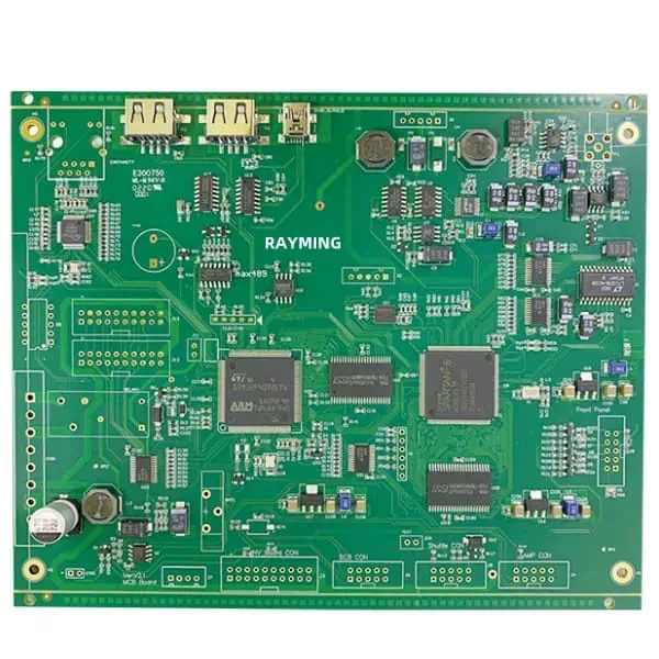
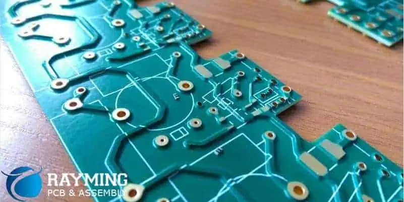
- RAYMING PCB: Known for their expertise in both standard and thick copper PCBs, offering cutting-edge technology and comprehensive design support.
- TTM Technologies: A global leader in PCB manufacturing with a wide range of capabilities.
- Wurth Elektronik: Specializes in complex PCB designs, including thick copper applications.
- AT&S: Offers advanced PCB solutions for various industries, including thick copper options.
- Millennium Circuits Limited: Provides a range of PCB services, including thick copper manufacturing.
Spotlight on RAYMING PCB
RAYMING PCB stands out as a top manufacturer in both standard and thick copper PCB production. Their key strengths include:
- Advanced Manufacturing Capabilities: State-of-the-art equipment for both standard and thick copper PCBs
- Comprehensive Design Support: Expert assistance in optimizing designs for manufacturability
- Quality Control: Rigorous testing and inspection processes to ensure high-quality products
- Flexibility: Ability to handle both high-volume production and specialized, low-volume orders
- Innovation: Continuous investment in research and development to stay at the forefront of PCB technology
Future Trends in PCB Technology
As technology continues to evolve, several trends are shaping the future of PCB manufacturing:
- Increased Integration: More complex, higher-density designs with embedded components
- Advanced Materials: Development of new substrate materials for improved performance
- 3D Printing: Exploration of additive manufacturing techniques for PCB production
- Flexible and Stretchable PCBs: Growing demand for wearable and conformable electronics
- Green Manufacturing: Focus on environmentally friendly materials and processes
Implications for Thick Copper PCBs
- Enhanced Power Density: Enabling more compact designs for high-power applications
- Improved Thermal Management: Development of new cooling solutions integrated with thick copper PCBs
- Hybrid Designs: Combining thick copper layers with standard layers for optimized performance
- Advanced Plating Technologies: Pushing the boundaries of copper thickness and uniformity
Frequently Asked Questions (FAQ)
1. What is the main difference between standard PCBs and thick copper PCBs?
The main difference lies in the thickness of the copper layers. Standard PCBs typically have copper thicknesses ranging from 0.5 oz to 2 oz (17.5 μm to 70 μm), while thick copper PCBs have copper thicknesses of 3 oz (105 μm) or more, sometimes reaching up to 20 oz (700 μm) or higher. This increased copper thickness allows thick copper PCBs to handle higher currents and provide better thermal management compared to standard PCBs.
2. When should I choose a thick copper PCB over a standard PCB?
You should consider using a thick copper PCB when your application requires:
- High current-carrying capacity
- Improved thermal management
- Enhanced durability and resistance to mechanical stress
- Better EMI/RFI shielding
- Reduced voltage drop in power distribution
Common applications include power electronics, high-current systems, LED lighting, aerospace and defense equipment, and industrial machinery.
3. Are thick copper PCBs more expensive than standard PCBs?
Yes, thick copper PCBs are generally more expensive than standard PCBs due to:
- More complex manufacturing processes
- Specialized equipment requirements
- Longer production times
- Higher material costs
However, the additional cost may be justified by the improved performance and reliability in high-power applications.
4. What are the design challenges associated with thick copper PCBs?
The main design challenges for thick copper PCBs include:
- Increased minimum trace width and spacing
- Limited aspect ratio for plated through-holes
- More complex impedance control
- Potential for board warpage due to uneven copper distribution
- Increased overall board thickness and weight
Designers need to account for these factors and may need to use specialized design tools and techniques.
5. Can thick copper PCBs be combined with standard PCB layers in a single board?
Yes, it is possible to create hybrid designs that combine thick copper layers with standard copper layers in a single PCB. This approach allows for optimized performance, balancing the benefits of thick copper in power and ground planes with the finer trace capabilities of standard copper layers for signal routing. However, such designs require careful planning and may have higher manufacturing complexity and cost.
In conclusion, the choice between standard PCBs and thick copper PCBs depends on the specific requirements of your application. While standard PCBs are suitable for a wide range of electronic devices, thick copper PCBs offer significant advantages in high-power and high-reliability applications. By understanding the characteristics, advantages, and limitations of each type, engineers and manufacturers can make informed decisions to optimize their electronic designs for performance, reliability, and cost-effectiveness.