High-Density Interconnect (HDI) Printed Circuit Boards (PCBs) have revolutionized the electronics industry, enabling the creation of smaller, lighter, and more powerful devices. As technology continues to advance, the demand for increasingly complex HDI PCB stackups has grown. This article explores the world of HDI PCB manufacturing, focusing on stackups ranging from 1+N+1 to 4+N+4, and the one-stop manufacturing solutions that make these intricate designs possible.
Understanding HDI PCB Stackups
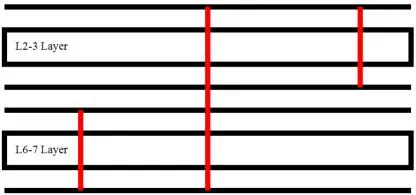
What is an HDI PCB?
HDI PCBs are characterized by their high wiring density and sophisticated interconnection structures. They typically feature:
- Microvias with diameters less than 150 microns
- High-density traces
- Fine-pitch components
- Multiple layers
Decoding HDI Stackup Notation
The notation used to describe HDI stackups (e.g., 1+N+1, 2+N+2, 3+N+3, 4+N+4) provides crucial information about the PCB’s structure:
- The first number represents the count of HDI layers on the top of the board
- “N” represents the number of standard (non-HDI) core layers
- The last number indicates the count of HDI layers on the bottom of the board
For example, a 2+N+2 stackup would have two HDI layers on top, N core layers, and two HDI layers on the bottom.
HDI PCB Stackup Configurations

1+N+1 Stackup
The 1+N+1 configuration is the simplest HDI stackup, featuring:
- One HDI layer on top
- N core layers
- One HDI layer on bottom
This stackup is suitable for designs that require moderate density and complexity.
2+N+2 Stackup
The 2+N+2 configuration offers increased routing capabilities:
- Two HDI layers on top
- N core layers
- Two HDI layers on bottom
This stackup allows for more complex routing and higher component density.
3+N+3 Stackup
The 3+N+3 configuration provides even greater design flexibility:
- Three HDI layers on top
- N core layers
- Three HDI layers on bottom
This stackup is ideal for designs requiring high component density and intricate routing.
4+N+4 Stackup
The 4+N+4 configuration represents the pinnacle of HDI complexity:
- Four HDI layers on top
- N core layers
- Four HDI layers on bottom
This stackup is used for the most demanding applications, offering maximum routing capabilities and component density.
Manufacturing Processes for HDI PCBs
Core Layer Fabrication
The manufacturing process for HDI PCBs begins with the fabrication of the core layers:
- Material selection
- Copper foil lamination
- Drilling
- Plating
- Etching
HDI Layer Build-Up
The HDI layers are then built up on the core:
- Lamination of thin dielectric material
- Laser drilling of microvias
- Electroless copper plating
- Electrolytic copper plating
- Photoresist application and exposure
- Developing and etching
Sequential Lamination
For more complex stackups (2+N+2, 3+N+3, 4+N+4), the process of adding HDI layers is repeated sequentially:
- Laminate additional dielectric layer
- Drill and plate microvias
- Pattern and etch copper
- Repeat for each additional HDI layer
Key Technologies in HDI PCB Manufacturing
Laser Drilling
Laser drilling is crucial for creating the small-diameter microvias in HDI PCBs:
- CO2 lasers for organic materials
- UV lasers for copper and other metals
Laser Drilling Parameters
| Parameter | Typical Range |
| Pulse duration | 10-100 nanoseconds |
| Repetition rate | 10-100 kHz |
| Power | 10-100 W |
| Spot size | 50-150 μm |
Advanced Plating Techniques
HDI PCBs require sophisticated plating processes:
- Electroless copper plating
- Electrolytic copper plating
- Selective plating for different features
Fine-Line Etching
Achieving high-density traces requires advanced etching techniques:
- Differential etching
- Additive processes
- Semi-additive processes
Design Considerations for HDI PCBs
Signal Integrity
Maintaining signal integrity is crucial in HDI designs:
- Controlled impedance routing
- Proper stackup design for return paths
- Minimizing crosstalk and EMI
Power Integrity
Ensuring stable power delivery is essential:
- Proper power plane design
- Decoupling capacitor placement
- Power distribution network (PDN) analysis
Thermal Management
Managing heat in dense HDI designs is critical:
- Thermal via placement
- Copper coin technology
- Embedded heat spreaders
One-Stop HDI PCB Manufacturing Solutions
Advantages of One-Stop Manufacturing
One-stop HDI PCB manufacturing offers several benefits:
- Streamlined production process
- Reduced time-to-market
- Improved quality control
- Cost-effectiveness
- Enhanced communication and problem-solving
Key Components of One-Stop HDI PCB Manufacturing
A comprehensive one-stop HDI PCB manufacturing solution should include:
- Design for Manufacturing (DFM) review
- Material selection and procurement
- Core layer fabrication
- HDI layer build-up
- Assembly and testing
- Quality assurance
Advanced Equipment for One-Stop HDI Manufacturing
Modern one-stop HDI PCB manufacturing facilities utilize state-of-the-art equipment:
Equipment List
| Equipment Type | Function |
| Laser drilling machines | Microvia formation |
| Direct imaging systems | High-precision patterning |
| Automated optical inspection (AOI) | Quality control |
| Flying probe testers | Electrical testing |
| X-ray inspection systems | Internal structure verification |
Challenges in HDI PCB Manufacturing

Microvia Reliability
Ensuring the reliability of microvias is crucial:
- Proper aspect ratio design
- Careful material selection
- Optimized plating processes
Registration Accuracy
Maintaining precise alignment between layers is critical:
- Advanced imaging systems
- Fiducial marks
- Compensation for material movement
Yield Optimization
Maximizing yield in HDI PCB production requires:
- Robust design rules
- Process control
- Continuous improvement initiatives
Future Trends in HDI PCB Manufacturing
Increased Density and Complexity
The trend towards higher density and complexity is expected to continue:
- Smaller microvia diameters
- Finer line widths and spacings
- More complex stackup configurations (e.g., 5+N+5)
Advanced Materials
New materials are being developed to meet the demands of future HDI PCBs:
- Low-loss materials for high-frequency applications
- Thermally conductive dielectrics
- Environmentally friendly substrate materials
Automation and Industry 4.0
The integration of automation and smart manufacturing principles will shape the future of HDI PCB production:
- AI-driven process optimization
- Real-time monitoring and adjustment
- Predictive maintenance
Conclusion
One-stop HDI PCB manufacturing of stackups from 1+N+1 to 4+N+4 represents the cutting edge of PCB technology. As electronic devices continue to evolve, demanding ever-higher levels of miniaturization and performance, the importance of advanced HDI PCB manufacturing capabilities will only grow. By leveraging state-of-the-art technologies and comprehensive one-stop solutions, manufacturers can meet the challenges of producing these complex boards while delivering high-quality, reliable products to market quickly and cost-effectively.
Frequently Asked Questions (FAQ)
Q1: What are the main advantages of HDI PCBs compared to traditional PCBs?
A1: HDI PCBs offer several advantages over traditional PCBs:
- Higher component density, allowing for smaller device sizes
- Improved electrical performance due to shorter signal paths
- Better signal integrity and reduced EMI
- Enhanced thermal management capabilities
- Increased design flexibility for complex circuits
Q2: How do manufacturers ensure the reliability of microvias in HDI PCBs?
A2: Manufacturers ensure microvia reliability through:
- Careful design of microvia aspect ratios
- Selection of appropriate materials for the application
- Optimized plating processes to ensure uniform copper deposition
- Rigorous testing procedures, including thermal cycling and reliability testing
- Continuous process monitoring and improvement
Q3: What are the key challenges in manufacturing 4+N+4 HDI PCBs?
A3: The main challenges in manufacturing 4+N+4 HDI PCBs include:
- Maintaining precise registration between multiple HDI layers
- Ensuring uniform plating of deep stacked microvias
- Managing thermal stress in the complex stackup
- Achieving high yields despite the increased complexity
- Balancing performance requirements with cost considerations
Q4: How does one-stop HDI PCB manufacturing benefit customers?
A4: One-stop HDI PCB manufacturing offers several benefits to customers:
- Reduced time-to-market due to streamlined production processes
- Improved quality control through integrated manufacturing stages
- Cost savings from optimized production and reduced logistics
- Enhanced problem-solving capabilities with a single point of contact
- Greater flexibility in design modifications and revisions
Q5: What future developments can we expect in HDI PCB technology?
A5: Future developments in HDI PCB technology may include:
- Even higher density stackups, such as 5+N+5 or beyond
- Incorporation of advanced materials for improved electrical and thermal performance
- Integration of embedded components within HDI layers
- Adoption of additive manufacturing techniques for certain PCB features
- Implementation of AI and machine learning for process optimization and quality control