Introduction
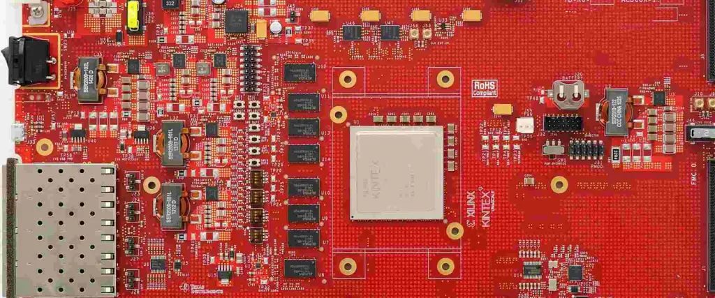
The XCKU060-1FFVA1517I is a high-performance Field-Programmable Gate Array (FPGA) from Xilinx’s Kintex UltraScale family. This powerful device offers an excellent balance of performance, power efficiency, and cost-effectiveness, making it ideal for a wide range of applications in telecommunications, data centers, medical imaging, and more. In this comprehensive guide, we’ll explore the key features, specifications, pinout details, and design considerations for the XCKU060-1FFVA1517I.
Overview of the Xilinx Kintex UltraScale FPGA Family
The UltraScale Architecture
The Xilinx Kintex UltraScale FPGA family, including the XCKU060-1FFVA1517I, is built on the advanced UltraScale architecture. This architecture offers significant improvements over previous generations, providing enhanced performance, reduced power consumption, and increased design flexibility.
Key Features of Kintex UltraScale FPGAs
- High-performance DSP slices
- Increased memory bandwidth
- Improved clock management
- Enhanced security features
- Scalable interconnect technology
XCKU060-1FFVA1517I Specifications
Device Overview
The XCKU060-1FFVA1517I is a mid-range device within the Kintex UltraScale family, offering a balance of resources suitable for a variety of applications.
Key Specifications
- Logic Cells: 725,550
- CLB Flip-Flops: 663,360
- CLB LUTs: 331,680
- Maximum Distributed RAM (Mb): 10.9
- Block RAM Blocks: 1,080
- Total Block RAM (Mb): 38.9
- UltraRAM Blocks: 0
- DSP Slices: 2,760
- CMTs: 12
- Maximum HP I/O: 520
- Maximum HD I/O: 96
- System Monitor: 1
Package Information
The XCKU060-1FFVA1517I comes in an FFVA1517 package, which is a flip-chip fine-pitch ball grid array (BGA) package with 1,517 pins.
Datasheet Highlights
Power Management
The XCKU060-1FFVA1517I features advanced power management capabilities, including:
- Multiple Power Domains: Allows for fine-grained control of power consumption
- Power Gating: Ability to shut down unused portions of the chip
- Intelligent Clock Gating: Reduces dynamic power consumption
Clock Management
Efficient clock management is crucial for high-performance designs. The XCKU060-1FFVA1517I offers:
- Mixed-Mode Clock Managers (MMCMs): 12 MMCMs for flexible clock synthesis and manipulation
- Phase-Locked Loops (PLLs): 24 PLLs for precise clock synchronization
- Global Clock Buffers: 544 global clock buffers for distributing clock signals
I/O Capabilities
The device provides versatile I/O options to support various interfaces:
- High-Performance (HP) I/O: Up to 520 user I/O pins
- High-Density (HD) I/O: Up to 96 user I/O pins
- GTH Transceivers: 48 GTH transceivers supporting up to 16.3 Gb/s
Read more about:
Pinout Details
Pin Configuration
The FFVA1517 package used by the XCKU060-1FFVA1517I has a 40 x 40 ball grid array layout. The pins are arranged in a manner that optimizes signal integrity and minimizes crosstalk.
I/O Bank Organization
The I/O pins are organized into banks, each supporting different voltage standards:
- HP I/O Banks: Support a wide range of single-ended and differential I/O standards
- HD I/O Banks: Offer high-density connectivity for memory interfaces and other applications
- GTH Transceiver Banks: Provide high-speed serial connectivity
Power Supply Pins
The XCKU060-1FFVA1517I requires multiple power supply voltages for different parts of the chip:
- VCCINT: Core voltage supply
- VCCAUX: Auxiliary voltage supply
- VCCBRAM: Block RAM supply voltage
- VCCIO: I/O bank supply voltage (varies depending on I/O standard)
Ground Pins
Proper grounding is essential for signal integrity and power distribution. The XCKU060-1FFVA1517I has numerous ground pins distributed across the package.
Design Guide
Design Flow Overview
Designing with the XCKU060-1FFVA1517I involves several key steps:
- Requirements Analysis: Define the project requirements and constraints
- Architecture Design: Create a high-level design of the system
- RTL Development: Write the VHDL or Verilog code for the design
- Synthesis: Convert the RTL code into a netlist of FPGA primitives
- Implementation: Place and route the design on the FPGA fabric
- Timing Analysis: Verify that the design meets timing requirements
- Bitstream Generation: Create the configuration file for the FPGA
Tools and Software
Xilinx provides a comprehensive suite of tools for designing with the XCKU060-1FFVA1517I:
- Vivado Design Suite: The primary integrated development environment (IDE) for UltraScale FPGAs
- Vitis: Unified software platform for developing embedded software and accelerated applications
- System Generator for DSP: High-level tool for DSP design on FPGAs
Best Practices for High-Performance Design
To achieve optimal performance with the XCKU060-1FFVA1517I, consider the following best practices:
- Efficient Use of DSP Slices: Leverage the high-performance DSP slices for arithmetic operations
- Memory Optimization: Use the appropriate mix of distributed RAM, block RAM, and UltraRAM
- Clock Domain Management: Carefully plan and implement clock domains to minimize skew and maximize performance
- Power Optimization: Utilize power gating and clock gating features to reduce power consumption
- I/O Planning: Carefully plan I/O assignments to minimize signal crosstalk and maximize signal integrity
Debugging and Verification
Xilinx provides several features and tools to aid in debugging and verifying designs on the XCKU060-1FFVA1517I:
- Integrated Logic Analyzer (ILA): On-chip debug tool for real-time signal monitoring
- Virtual I/O (VIO): Allows for dynamic probing and control of internal signals
- Vivado Simulator: Integrated simulator for functional and timing simulation
- Hardware Manager: Tool for programming and interacting with the FPGA
Application Areas
The XCKU060-1FFVA1517I is suitable for a wide range of applications, including:
- Telecommunications: 5G infrastructure, network processing, and packet processing
- Data Centers: Network interface cards, storage controllers, and compute acceleration
- Medical Imaging: Image processing and analysis for MRI, CT, and ultrasound systems
- Industrial Automation: Motion control, robotics, and machine vision
- Aerospace and Defense: Radar systems, electronic warfare, and secure communications
Performance Benchmarks
DSP Performance
The XCKU060-1FFVA1517I excels in DSP-intensive applications:
- Symmetric FIR Filter: Up to 2,760 GMACs (Giga Multiply-Accumulate operations per second)
- FFT Performance: Capable of processing large FFTs with low latency
Memory Bandwidth
With its extensive memory resources, the XCKU060-1FFVA1517I offers impressive memory bandwidth:
- Block RAM: Up to 4,503 Gb/s peak bandwidth
- Distributed RAM: Additional low-latency memory option for small data structures
Transceiver Performance
The GTH transceivers in the XCKU060-1FFVA1517I support high-speed serial communication:
- Maximum Data Rate: Up to 16.3 Gb/s per transceiver
- Aggregate Bandwidth: Up to 782.4 Gb/s (48 transceivers)
Comparison with Other Kintex UltraScale Devices
XCKU060-1FFVA1517I vs. XCKU040
- Logic Cells: XCKU060 has 725,550 vs. XCKU040’s 530,250
- DSP Slices: XCKU060 has 2,760 vs. XCKU040’s 1,920
- Block RAM: XCKU060 has 38.9 Mb vs. XCKU040’s 21.1 Mb
XCKU060-1FFVA1517I vs. XCKU095
- Logic Cells: XCKU060 has 725,550 vs. XCKU095’s 1,176,000
- DSP Slices: XCKU060 has 2,760 vs. XCKU095’s 4,100
- Block RAM: XCKU060 has 38.9 Mb vs. XCKU095’s 54.8 Mb
Conclusion
The XCKU060-1FFVA1517I Xilinx Kintex UltraScale FPGA offers a powerful and flexible platform for a wide range of high-performance applications. With its balanced mix of logic, memory, and DSP resources, coupled with high-speed transceivers and advanced power management features, this device is well-suited for demanding tasks in telecommunications, data centers, medical imaging, and more.
By leveraging the comprehensive tools provided by Xilinx and following best design practices, engineers can fully utilize the capabilities of the XCKU060-1FFVA1517I to create innovative and efficient solutions. As the demand for high-performance, low-power computing continues to grow, the XCKU060-1FFVA1517I stands as a compelling choice for designers looking to push the boundaries of what’s possible with FPGA technology.