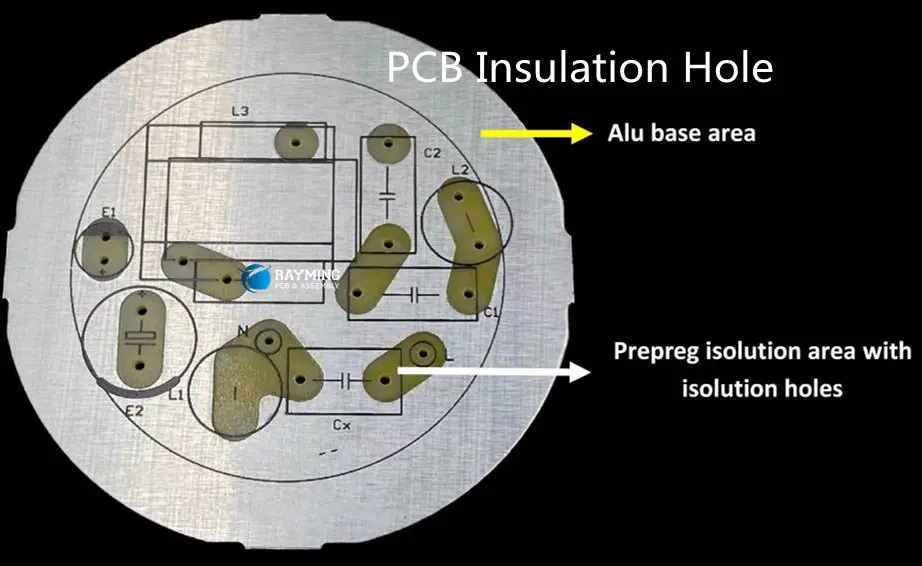
Inner layer pad insulation is a crucial component in the construction of printed circuit boards (PCBs), playing a vital role in the overall performance and reliability of electronic devices. This specialized material is designed to provide electrical insulation, thermal management, and structural support within the complex layered structure of multilayer PCBs.
As electronic devices continue to shrink in size while simultaneously increasing in functionality and power, the importance of effective insulation between conductive layers becomes paramount. Inner layer pad insulation addresses this need by creating a barrier between copper layers, preventing short circuits and ensuring the proper functioning of the circuit.
In this comprehensive article, we will explore the various aspects of inner layer pad insulation, including its composition, manufacturing processes, properties, applications, and impact on PCB performance. We will also discuss the latest developments in this field and how they are shaping the future of electronics.
Composition and Types of Inner Layer Pad Insulation
Basic Components
Inner layer pad insulation materials are typically composed of a combination of the following elements:
- Base material: Usually a type of polymer or resin
- Reinforcing fibers: Glass fibers or other strengthening materials
- Flame retardants: Additives to improve fire resistance
- Fillers: Materials to enhance specific properties such as thermal conductivity or dimensional stability
Common Types of Inner Layer Pad Insulation
There are several types of materials used for inner layer pad insulation in PCBs. The choice of material depends on various factors, including the specific application, performance requirements, and cost considerations. Here are some of the most common types:
1. FR-4 (Flame Retardant 4)
FR-4 is the most widely used material for PCB substrates and inner layer insulation. It consists of a woven fiberglass cloth impregnated with an epoxy resin system.
Advantages:
- Good electrical insulation properties
- Excellent mechanical strength
- Flame retardant
- Relatively low cost
Disadvantages:
- Limited high-frequency performance
- Moisture absorption can be an issue in some applications
2. Polyimide
Polyimide is a high-performance polymer known for its excellent thermal stability and electrical properties.
Advantages:
- Exceptional heat resistance
- Low dielectric constant and loss tangent
- Good dimensional stability
- Suitable for flex and rigid-flex applications
Disadvantages:
- Higher cost compared to FR-4
- Can be challenging to process
3. PTFE (Polytetrafluoroethylene)
PTFE, also known by the brand name Teflon, is used in high-frequency and high-speed applications.
Advantages:
- Excellent electrical properties at high frequencies
- Very low moisture absorption
- Good chemical resistance
Disadvantages:
- Expensive
- Requires specialized processing techniques
4. Ceramic-filled PTFE
This material combines PTFE with ceramic fillers to enhance certain properties.
Advantages:
- Improved dimensional stability compared to pure PTFE
- Better thermal conductivity
- Maintains excellent electrical properties
Disadvantages:
- Higher cost than standard PTFE
- Can be brittle and require careful handling
5. BT (Bismaleimide Triazine) Resin
BT resin is an advanced thermoset polymer used in high-performance PCBs.
Advantages:
- Low dielectric constant and loss tangent
- Good thermal stability
- Better dimensional stability than FR-4
Disadvantages:
- More expensive than FR-4
- Can be brittle and require careful processing
Manufacturing Process of Inner Layer Pad Insulation
The manufacturing process for inner layer pad insulation is a critical step in PCB production. The process varies depending on the type of material used, but generally follows these steps:
1. Material Preparation
- Raw materials (resins, reinforcing fibers, additives) are carefully selected and mixed according to the desired formulation.
- For composite materials like FR-4, fiberglass cloth is prepared in large rolls.
2. Impregnation
- For materials like FR-4, the fiberglass cloth is passed through a bath of liquid resin.
- The resin impregnates the cloth, coating the fibers and filling the spaces between them.
3. B-Staging
- The impregnated material is partially cured in an oven, creating what is known as “prepreg” (pre-impregnated) material.
- This B-staged material is easier to handle and can be stored for later use.
4. Cutting and Layup
- The prepreg material is cut to the required size for the PCB.
- Multiple layers of prepreg are stacked alternately with copper foil layers to create the PCB structure.
5. Lamination
- The layered stack is placed in a lamination press.
- Heat and pressure are applied to fully cure the resin and bond all layers together.
6. Drilling and Plating
- After lamination, holes are drilled through the board for vias and component leads.
- The holes are then plated with copper to create electrical connections between layers.
7. Etching and Patterning
- The outer copper layers are etched to create the desired circuit pattern.
- Inner layer circuits are typically etched before lamination.
8. Final Processing
- Additional layers such as solder mask and silkscreen are applied.
- The board undergoes final testing and inspection.
This process creates a multilayer PCB with inner layer pad insulation integrated into its structure. The insulation material provides electrical isolation between conductive layers while also contributing to the overall mechanical and thermal properties of the board.
Properties and Characteristics of Inner Layer Pad Insulation
The effectiveness of inner layer pad insulation is determined by several key properties. These characteristics influence the performance, reliability, and suitability of the PCB for specific applications. Let’s examine the most important properties:
1. Dielectric Constant (Dk)
The dielectric constant, also known as relative permittivity, is a measure of the material’s ability to store electrical energy in an electric field.
- Lower Dk values generally result in faster signal propagation and less signal loss.
- Typical Dk values range from about 3.0 to 4.5 for common PCB materials.
2. Dissipation Factor (Df)
Also known as the loss tangent, the dissipation factor indicates the amount of energy lost as heat in the insulation material.
- Lower Df values result in less signal attenuation and are preferred for high-frequency applications.
- Common PCB materials have Df values ranging from 0.002 to 0.02.
3. Thermal Conductivity
This property measures the material’s ability to conduct heat.
- Higher thermal conductivity helps dissipate heat from components and traces.
- Values typically range from 0.2 to 1.0 W/m·K for PCB insulation materials.
4. Coefficient of Thermal Expansion (CTE)
CTE describes how the material’s dimensions change with temperature.
- Matching the CTE of the insulation to that of copper and components helps prevent stress and failure during thermal cycling.
- CTE is often different in the x-y plane versus the z-axis due to the presence of reinforcing fibers.
5. Glass Transition Temperature (Tg)
Tg is the temperature at which the material transitions from a rigid to a more flexible state.
- Higher Tg values indicate better performance at elevated temperatures.
- Common Tg values range from 130°C to over 200°C for high-performance materials.
6. Decomposition Temperature (Td)
Td is the temperature at which the material begins to break down chemically.
- Higher Td values indicate better resistance to extreme temperatures and processes like lead-free soldering.
- Td values typically range from 300°C to over 400°C for high-performance materials.
7. Moisture Absorption
This property indicates how much moisture the material absorbs from its environment.
- Lower moisture absorption is generally preferred to maintain stable electrical and mechanical properties.
- Values typically range from less than 0.1% to about 0.5% for common PCB materials.
8. Dielectric Strength
Dielectric strength measures the maximum electric field the material can withstand without breaking down.
- Higher values indicate better insulation properties.
- Typical values range from 20 to 60 kV/mm for PCB insulation materials.
9. Flexural Strength
This property measures the material’s ability to resist deformation under load.
- Higher flexural strength indicates better mechanical durability.
- Values typically range from 300 to 500 MPa for common PCB materials.
To better visualize these properties, let’s look at a comparison table of some common inner layer pad insulation materials:
| Property | FR-4 | Polyimide | PTFE | BT Resin |
| Dielectric Constant (Dk) | 4.0-4.5 | 3.2-3.5 | 2.1-2.5 | 3.5-3.9 |
| Dissipation Factor (Df) | 0.015-0.020 | 0.002-0.005 | 0.0002-0.0005 | 0.005-0.010 |
| Thermal Conductivity (W/m·K) | 0.3-0.5 | 0.3-0.5 | 0.2-0.3 | 0.3-0.4 |
| CTE (ppm/°C) (x-y / z) | 14-17 / 50-70 | 12-16 / 40-50 | 70-280 / 250-300 | 13-15 / 40-50 |
| Glass Transition Temp (Tg) (°C) | 130-180 | 250-260 | N/A | 180-220 |
| Decomposition Temp (Td) (°C) | 300-315 | 450-500 | 380-400 | 350-380 |
| Moisture Absorption (%) | 0.1-0.5 | 0.3-0.8 | <0.01 | 0.1-0.3 |
| Dielectric Strength (kV/mm) | 20-40 | 25-35 | 40-60 | 30-45 |
| Flexural Strength (MPa) | 300-500 | 350-450 | 10月20日 | 300-400 |
This table illustrates the range of properties available in different inner layer pad insulation materials, highlighting why certain materials are chosen for specific applications based on their unique characteristics.
Applications and Impact on PCB Performance
Inner layer pad insulation plays a crucial role in various PCB applications, significantly impacting the overall performance and reliability of electronic devices. Let’s explore some key applications and how inner layer pad insulation affects PCB performance:
High-Frequency and High-Speed Applications
In applications such as telecommunications, aerospace, and high-performance computing, inner layer pad insulation is critical for maintaining signal integrity.
Impact on Performance:
- Low Dk and Df materials minimize signal loss and distortion.
- Controlled impedance is easier to achieve with consistent insulation properties.
- Reduced crosstalk between adjacent traces due to better insulation.
Power Electronics
Power electronic devices, including power supplies, motor drives, and inverters, rely heavily on effective insulation between high-voltage components.
Impact on Performance:
- High dielectric strength prevents breakdown under high voltages.
- Good thermal conductivity helps dissipate heat from power components.
- Materials with high Tg and Td withstand the higher temperatures associated with power electronics.
Automotive Electronics
The harsh environment and reliability requirements of automotive electronics demand robust insulation materials.
Impact on Performance:
- Resistance to thermal cycling prevents delamination and cracking.
- Low moisture absorption maintains consistent performance in varying humidity conditions.
- Flame retardant properties enhance safety in the event of a vehicle fire.
Aerospace and Defense
These industries require PCBs that can withstand extreme conditions while maintaining high reliability.
Impact on Performance:
- Materials with low outgassing properties are suitable for space applications.
- High thermal stability ensures consistent performance across a wide temperature range.
- Excellent dimensional stability prevents warpage and misalignment in critical systems.
Medical Devices
Medical electronics often require biocompatibility and the ability to withstand sterilization processes.
Impact on Performance:
- Materials resistant to chemicals used in sterilization processes maintain integrity.
- Low moisture absorption prevents performance changes in high-humidity environments.
- Consistent electrical properties ensure reliable operation of sensitive medical equipment.
Internet of Things (IoT) Devices
As IoT devices become smaller and more ubiquitous, the role of inner layer pad insulation becomes increasingly important.
Impact on Performance:
- Thin, high-performance materials allow for miniaturization without compromising functionality.
- Low Dk materials support the high-frequency communications often used in IoT devices.
- Materials with good thermal management properties help dissipate heat in compact designs.
5G and Beyond
The rollout of 5G networks and development of future communication technologies place new demands on PCB materials.
Impact on Performance:
- Extremely low loss materials are essential for minimizing signal attenuation at millimeter-wave frequencies.
- Consistent Dk across a wide frequency range ensures predictable performance.
- Materials with low moisture sensitivity maintain stable performance in outdoor installations.
Recent Developments and Future Trends
The field of inner layer pad insulation is continuously evolving to meet the growing demands of the electronics industry. Here are some recent developments and future trends:
1. Advanced Composite Materials
Researchers and manufacturers are developing new composite materials that combine the benefits of different insulation types.
Example: Hybrid materials that incorporate both ceramic and polymer components to achieve optimal electrical and thermal properties.
2. Nanotechnology-Enhanced Insulation
The integration of nanomaterials into traditional insulation materials is opening up new possibilities for performance enhancement.
Example: Carbon nanotubes or graphene added to epoxy resins to improve thermal conductivity and mechanical strength.
3. Eco-Friendly and Sustainable Materials
There is a growing focus on developing insulation materials that are more environmentally friendly and sustainable.
Example: Bio-based epoxy resins derived from renewable resources, reducing the reliance on petroleum-based products.
4. Ultra-Low Loss Materials
For applications in 5G, 6G, and beyond, there is a push to develop materials with extremely low dielectric loss.
Example: Advanced PTFE composites with Df values below 0.0010 across a wide frequency range.
5. Adaptive and Smart Materials
Research is being conducted on insulation materials that can adapt their properties in response to environmental conditions.
Example: Materials that can change their thermal conductivity based on temperature, improving heat management in variable load conditions.
6. 3D Printable Insulation Materials
As additive manufacturing techniques for electronics advance, there is interest in developing inner layer pad insulation materials suitable for 3D printing.
Example: Specialized resins that can be 3D printed and cured to form complex, multi-material PCB structures.
7. Integration of Functional Properties
Future insulation materials may incorporate additional functionalities beyond traditional electrical and thermal properties.
Example: Insulation layers with built-in EMI shielding or self-healing capabilities to improve long-term reliability.
8. Artificial Intelligence in Material Design
AI and machine learning techniques are being applied to accelerate the development and optimization of new insulation materials.
Example: Using AI to predict material properties and performance, reducing the time and cost of experimental testing.
Conclusion
Inner layer pad insulation is a critical component in the design and manufacture of modern PCBs, playing a vital role in the performance, reliability, and miniaturization of electronic devices. As we’ve explored in this article, the choice of insulation material impacts various aspects of PCB performance, from signal integrity and thermal management to mechanical durability and environmental resistance.
The field of inner layer pad insulation continues to evolve, driven by the demands of emerging technologies such as 5G, IoT, and advanced computing systems. Innovations in material science, nanotechnology, and manufacturing processes are pushing the boundaries of what’s possible in PCB design and performance.
As electronic devices become increasingly integrated into every aspect of our lives, the importance of high-quality, reliable inner layer pad insulation will only grow. Engineers and designers must stay informed about the latest developments in this field to create the next generation of electronic products that are faster, smaller, more efficient, and more reliable than ever before.