Introduction
LED grow lights have revolutionized indoor farming and horticulture, offering energy-efficient and customizable lighting solutions for plants. At the heart of these innovative lighting systems lies the printed circuit board (PCB), which serves as the foundation for mounting and connecting the LED components. This comprehensive guide delves into the intricate world of LED grow light PCB manufacturing, covering everything from design considerations to material selection and production processes.
Understanding LED Grow Lights
Before diving into the manufacturing process, it’s essential to understand the basics of LED grow lights and their importance in modern agriculture.
What are LED Grow Lights?
LED grow lights are specialized lighting fixtures designed to stimulate plant growth by emitting light at specific wavelengths that plants need for photosynthesis and other biological processes. These lights offer several advantages over traditional lighting solutions:
- Energy efficiency
- Longer lifespan
- Reduced heat output
- Customizable light spectra
- Compact design
The Role of PCBs in LED Grow Lights
Printed Circuit Boards (PCBs) play a crucial role in LED grow lights by:
- Providing a stable mounting surface for LEDs
- Facilitating electrical connections between components
- Managing heat dissipation
- Enabling complex circuit designs for advanced features
- Ensuring consistent light output and performance
PCB Basics for LED Grow Lights
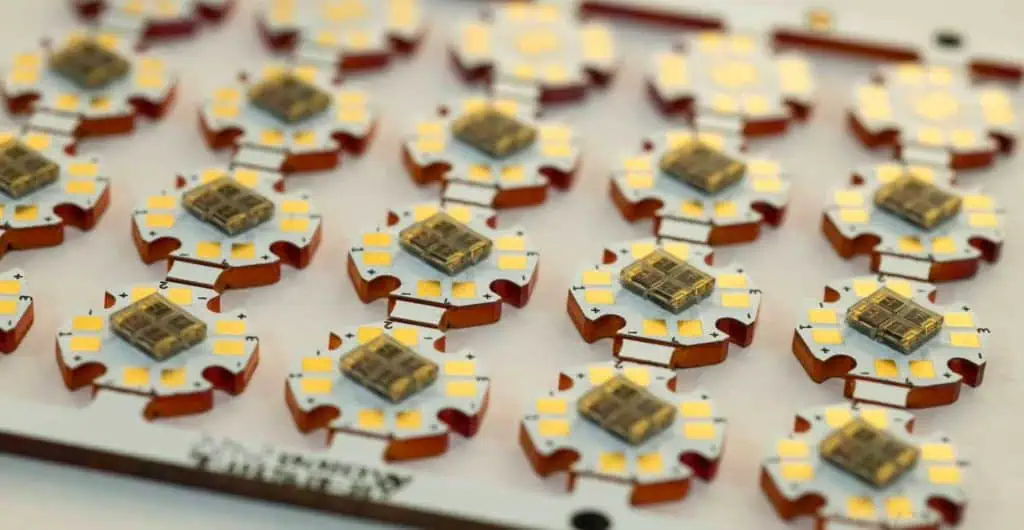
Types of PCBs Used in LED Grow Lights
LED grow light PCBs come in various types, each with its own set of advantages and applications:
- Single-sided PCBs
- Double-sided PCBs
- Multi-layer PCBs
- Metal-core PCBs (MCPCBs)
- Flexible PCBs
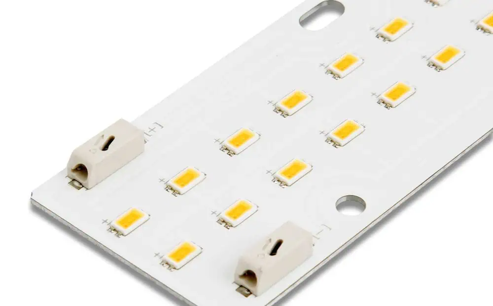
Key Components of LED Grow Light PCBs
A typical LED grow light PCB consists of several essential components:
- LEDs (Light Emitting Diodes)
- Resistors
- Capacitors
- Drivers
- Connectors
- Heat sinks
- Thermal management materials
Designing LED Grow Light PCBs
Designing an effective LED grow light PCB requires careful consideration of various factors to ensure optimal performance and longevity.
Design Considerations
- Light Output and Spectrum: Determine the desired light intensity and spectral composition based on the target plants and growth stages.
- Thermal Management: Implement effective heat dissipation strategies to prevent LED degradation and maintain efficiency.
- Power Distribution: Design proper power distribution to ensure consistent performance across all LEDs.
- Circuit Protection: Incorporate protection mechanisms against voltage spikes, short circuits, and other electrical issues.
- Modularity: Consider modular designs for easier maintenance and upgradability.
- Compliance: Ensure the design meets relevant safety and regulatory standards.
PCB Layout Best Practices
- Component Placement: Optimize LED placement for even light distribution and efficient heat dissipation.
- Trace Width and Spacing: Use appropriate trace widths to handle current requirements and maintain proper spacing for thermal management.
- Ground Plane: Implement a solid ground plane for improved electrical performance and heat distribution.
- Thermal Vias: Incorporate thermal vias to enhance heat transfer from the LED junction to the heat sink.
- Silkscreen and Markings: Include clear markings for component placement, polarity, and other essential information.
Material Selection for LED Grow Light PCBs
Choosing the right materials for LED grow light PCBs is crucial for ensuring performance, durability, and thermal management.
PCB Substrate Materials
| Material | Thermal Conductivity (W/mK) | Dielectric Constant | Advantages | Disadvantages |
|---|---|---|---|---|
| FR-4 | 0.3 – 0.5 | 4.2 – 5.0 | Low cost, widely available | Limited thermal performance |
| Aluminum | 150 – 200 | N/A (metal core) | Excellent thermal management | Higher cost, requires special processing |
| Ceramic | 20 – 170 | 9.0 – 10.0 | High thermal conductivity, low CTE | Brittle, expensive |
| Polyimide | 0.12 – 0.28 | 3.2 – 3.5 | Flexible, high-temperature resistance | Lower thermal conductivity |
Copper Foil Thickness
The thickness of the copper foil used in PCB manufacturing affects both electrical and thermal performance:
| Copper Thickness | Weight (oz/ft²) | Current Carrying Capacity | Heat Dissipation |
|---|---|---|---|
| 1 oz | 1 | Moderate | Standard |
| 2 oz | 2 | Higher | Improved |
| 3 oz | 3 | Very high | Excellent |
Solder Mask and Silkscreen
- Solder Mask: Choose a high-quality, heat-resistant solder mask to protect the PCB from environmental factors and improve insulation.
- Silkscreen: Opt for clear, heat-resistant silkscreen inks for component markings and other essential information.
Manufacturing Process
The manufacturing process for LED grow light PCBs involves several steps, each crucial for producing high-quality, reliable boards.
Step-by-Step Manufacturing Process
- Design and File Preparation
- Finalize PCB design
- Generate Gerber files and other manufacturing data
- Material Selection and Preparation
- Choose appropriate substrate material
- Cut raw material to size
- Inner Layer Processing (for multi-layer PCBs)
- Apply photoresist
- Expose and develop inner layer patterns
- Etch copper
- Layer Alignment and Pressing
- Stack and align layers
- Apply prepreg material
- Press layers together under heat and pressure
- Drilling
- Drill holes for vias, component leads, and mounting
- Plating
- Apply electroless copper to coat hole walls
- Electroplate additional copper for desired thickness
- Outer Layer Imaging and Etching
- Apply photoresist to outer layers
- Expose and develop outer layer patterns
- Etch excess copper
- Solder Mask Application
- Apply solder mask material
- Expose and develop solder mask pattern
- Surface Finish
- Apply chosen surface finish (e.g., HASL, ENIG, OSP)
- Silkscreen Printing
- Print component markings and other information
- Electrical Testing
- Perform flying probe or fixture tests
- Cutting and Profiling
- Cut individual PCBs from panel
- Route or punch final board shape
- Final Inspection and Packaging
- Visual inspection
- Packaging for shipping
Advanced Manufacturing Techniques
- Laser Drilling: For high-precision, small-diameter holes
- Direct Imaging: For improved accuracy in pattern transfer
- Automated Optical Inspection (AOI): For enhanced quality control
- X-ray Inspection: For checking internal layers and hidden solder joints
Quality Control and Testing
Ensuring the quality and reliability of LED grow light PCBs is crucial for long-term performance and customer satisfaction.
Quality Control Measures
- Incoming Material Inspection: Verify the quality of raw materials before production
- In-Process Inspections: Regular checks during each stage of manufacturing
- Automated Optical Inspection (AOI): Detect defects in solder mask, silkscreen, and copper patterns
- X-ray Inspection: Examine internal layers and hidden solder joints
- Electrical Testing: Verify circuit continuity and isolation
Performance Testing
- Thermal Cycling: Test PCB performance under varying temperature conditions
- Vibration Testing: Ensure durability in high-vibration environments
- Humidity Testing: Verify resistance to moisture ingress
- Light Output Measurement: Confirm desired intensity and spectral distribution
- EMI/EMC Testing: Check for electromagnetic interference and compatibility
Cost Considerations
Understanding the factors that influence the cost of LED grow light PCB manufacturing can help in making informed decisions and optimizing production expenses.
Factors Affecting PCB Manufacturing Costs
| Factor | Impact on Cost | Considerations |
|---|---|---|
| Board Size | Larger boards increase cost | Optimize design for efficient space usage |
| Layer Count | More layers increase cost | Balance complexity with layer count |
| Material Selection | Specialty materials cost more | Choose materials based on performance requirements |
| Copper Weight | Heavier copper increases cost | Select appropriate weight for current and thermal needs |
| Surface Finish | Some finishes are more expensive | Consider durability and assembly method |
| Minimum Feature Size | Smaller features increase cost | Design with manufacturability in mind |
| Order Quantity | Larger quantities reduce per-unit cost | Consider production volume and inventory management |
| Turnaround Time | Faster production increases cost | Plan production schedule to balance cost and lead time |
Cost Optimization Strategies
- Design for Manufacturability (DFM): Optimize designs to reduce complexity and improve yield
- Panel Utilization: Maximize the number of PCBs per panel to reduce waste
- Material Selection: Choose cost-effective materials that meet performance requirements
- Volume Production: Leverage economies of scale for larger production runs
- Supplier Relationships: Develop long-term partnerships with PCB manufacturers for better pricing
Future Trends in LED Grow Light PCB Manufacturing
As technology advances, several trends are shaping the future of LED grow light PCB manufacturing:
- Increased Automation: Greater use of robotics and AI in PCB production
- Advanced Materials: Development of new substrate materials with improved thermal and electrical properties
- 3D Printing: Exploration of additive manufacturing techniques for PCB production
- IoT Integration: Incorporation of sensors and connectivity features in LED grow light PCBs
- Sustainable Manufacturing: Focus on eco-friendly materials and energy-efficient production processes
- Miniaturization: Trend towards smaller, more efficient LED grow light designs
- Flexible and Stretchable PCBs: Development of adaptable PCB solutions for unique grow light applications
Frequently Asked Questions
1. What is the best PCB material for LED grow lights?
The best PCB material for LED grow lights depends on the specific requirements of your application. For high-power LED grow lights that generate significant heat, metal-core PCBs (MCPCBs) made with aluminum substrates are often the preferred choice due to their excellent thermal management properties. For lower-power applications or where cost is a primary concern, FR-4 boards with additional thermal management features may be suitable.
2. How do I ensure proper thermal management in LED grow light PCBs?
Proper thermal management in LED grow light PCBs can be achieved through several strategies:
- Use of metal-core PCBs or boards with high thermal conductivity
- Incorporation of thermal vias to improve heat transfer
- Optimal component placement to distribute heat evenly
- Integration of heat sinks or cooling systems
- Selection of LEDs with good thermal properties
- Proper thermal design and simulation during the PCB layout phase
3. What surface finish is recommended for LED grow light PCBs?
The choice of surface finish depends on factors such as assembly method, environmental conditions, and cost considerations. Some popular options include:
- ENIG (Electroless Nickel Immersion Gold): Offers good solderability and protection against oxidation
- HASL (Hot Air Solder Leveling): Cost-effective option with good solderability
- OSP (Organic Solderability Preservative): Environmentally friendly option suitable for lead-free soldering
- Immersion Silver: Provides good solderability and conductivity
ENIG is often preferred for LED grow light PCBs due to its excellent surface planarity and protection against harsh environments.
4. How can I reduce the cost of LED grow light PCB manufacturing?
To reduce the cost of LED grow light PCB manufacturing, consider the following strategies:
- Optimize PCB design for manufacturability
- Choose cost-effective materials that meet performance requirements
- Increase order quantities to benefit from economies of scale
- Simplify the PCB design where possible (e.g., reduce layer count)
- Work closely with your PCB manufacturer to identify cost-saving opportunities
- Consider panel utilization to maximize the number of PCBs per production panel
- Balance performance requirements with cost considerations in material and process selection
5. What are the key differences between PCBs for LED grow lights and other LED applications?
While there are similarities, PCBs for LED grow lights have some unique considerations compared to other LED applications:
- Spectral Output: Grow light PCBs often require specific combinations of LED colors to achieve optimal light spectra for plant growth
- Higher Power Density: Grow lights typically operate at higher power levels, requiring robust thermal management
- Environmental Resistance: PCBs for grow lights must withstand high humidity and potentially harsh greenhouse conditions
- Customization: Grow light PCBs often need to be tailored for specific crop types or growth stages
- Longevity: With extended operation times, grow light PCBs require designs that ensure long-term reliability and performance