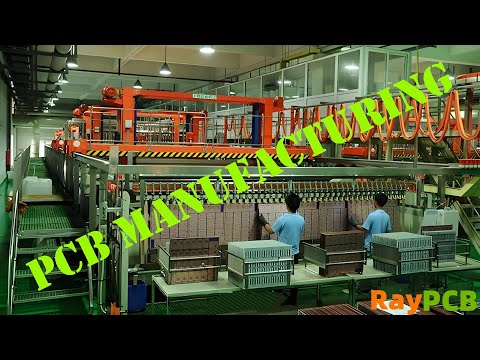
Gold plating represents one of the most critical surface finishing processes in printed circuit board (PCB) manufacturing, providing essential protection and functionality to electronic components. This sophisticated electrochemical process applies a thin layer of gold to specific areas of the PCB, creating a corrosion-resistant, highly conductive surface that ensures reliable electrical connections and long-term performance.
Understanding Gold Plating in PCB Manufacturing
Gold plating in PCB production serves multiple vital functions beyond mere aesthetics. The primary purpose involves creating oxidation-resistant contact surfaces that maintain excellent electrical conductivity over extended periods. Unlike copper, which readily oxidizes when exposed to air and moisture, gold remains chemically inert under normal environmental conditions, making it ideal for critical connection points such as edge connectors, component pads, and test points.
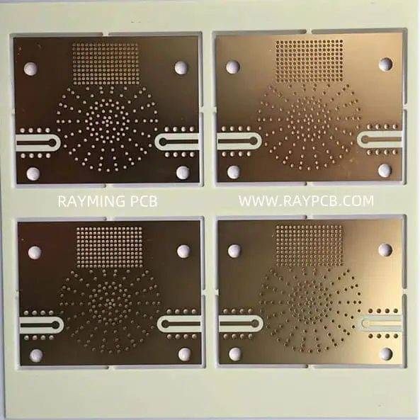
The gold plating process typically involves depositing a thin layer of gold, usually ranging from 0.05 to 2.54 microns (2 to 100 microinches) in thickness, onto designated areas of the PCB. This seemingly minimal thickness provides substantial protection while maintaining cost-effectiveness, as gold remains one of the more expensive materials used in PCB manufacturing.
Types of Gold Plating Processes
PCB manufacturers employ several distinct gold plating techniques, each suited to specific applications and requirements. Hard gold plating, also known as electrolytic gold plating, involves depositing a relatively thick layer of gold (typically 1.27 to 2.54 microns) that contains small amounts of hardening agents such as cobalt or nickel. This process creates a durable surface capable of withstanding repeated insertions and mechanical stress, making it ideal for edge connectors and switches.
Soft gold plating, conversely, deposits pure gold without hardening additives, resulting in a more malleable surface excellent for wire bonding applications. The thickness typically ranges from 0.25 to 1.27 microns, providing adequate protection while maintaining the material properties necessary for reliable wire bond connections.
Electroless nickel immersion gold (ENIG) represents another popular approach, combining a nickel barrier layer with a thin immersion gold coating. This process offers excellent planarity and is particularly well-suited for surface mount technology applications where component placement accuracy is crucial.
The Gold Plating Process Steps
The gold plating process begins with thorough PCB preparation, including cleaning to remove any contaminants, oxides, or residues that might interfere with proper adhesion. This cleaning typically involves both chemical and mechanical methods to ensure optimal surface condition.
Following cleaning, the PCB undergoes a nickel plating step, which serves as a barrier layer between the copper substrate and the gold coating. Nickel prevents copper migration into the gold layer, which could compromise the gold’s protective properties and electrical performance. The nickel layer typically ranges from 1.27 to 5.08 microns in thickness.
The actual gold plating occurs through electrochemical deposition, where the PCB serves as the cathode in an electrolytic cell containing gold cyanide or gold sulfite solutions. Electric current drives gold ions from the solution onto the PCB surface, creating a uniform, adherent coating. Process parameters such as current density, temperature, pH, and plating time must be carefully controlled to achieve consistent results.
Critical Process Parameters
Temperature control plays a crucial role in gold plating quality, with most processes operating between 60-70°C (140-158°F). Higher temperatures can accelerate deposition rates but may also increase the risk of poor adhesion or grain structure issues. Lower temperatures generally produce finer grain structures but require longer plating times.
Current density directly affects deposition rate and gold layer characteristics. Typical current densities range from 0.5 to 2.0 amperes per square decimeter, with higher densities producing faster deposition but potentially compromising surface quality. Maintaining uniform current distribution across the PCB surface ensures consistent gold thickness and quality.
Solution chemistry requires constant monitoring and adjustment to maintain optimal plating conditions. Gold concentration, pH levels, and the presence of organic additives all influence the final coating properties. Regular solution analysis and replenishment help maintain consistent plating quality throughout production runs.
Quality Control and Testing
Gold plating quality assessment involves multiple testing methods to ensure specification compliance. Thickness measurements using X-ray fluorescence or cross-sectional microscopy verify that gold deposits meet dimensional requirements across the entire PCB surface.
Adhesion testing evaluates the bond strength between the gold layer and underlying nickel or copper substrates. Standard tests include tape adhesion tests and thermal cycling to simulate operational stresses that might cause coating failure.
Solderability testing ensures that gold-plated surfaces maintain their ability to form reliable solder joints. This testing becomes particularly important for surfaces that will undergo multiple thermal cycles during assembly and rework operations.
Porosity testing identifies potential defects in the gold coating that could allow corrosive agents to reach the underlying metal layers. Various methods, including electrolytic porosity tests, help identify coating integrity issues before final product shipment.
Applications and Benefits
Gold plating finds extensive application in high-reliability electronic systems where connection integrity is paramount. Aerospace and defense electronics commonly specify gold plating for critical connections due to its exceptional corrosion resistance and long-term stability. Medical devices also frequently utilize gold plating to ensure reliable operation in challenging environments.
Consumer electronics benefit from gold plating in applications such as memory card contacts, USB connectors, and audio/video interfaces where repeated insertions occur. The superior wear resistance of hard gold plating makes these connections reliable throughout their intended service life.
The benefits of gold plating extend beyond corrosion protection to include excellent electrical conductivity, thermal stability, and biocompatibility. These properties make gold plating suitable for applications ranging from implantable medical devices to high-frequency RF circuits where signal integrity is crucial.
Challenges and Considerations
Despite its advantages, gold plating presents several challenges that manufacturers must address. Cost considerations often drive decisions about where to apply gold plating, as the material expense can significantly impact overall PCB costs. Selective plating techniques help minimize gold usage while maintaining performance in critical areas.
Environmental regulations increasingly affect gold plating processes, particularly regarding cyanide-based plating solutions. Many manufacturers have transitioned to more environmentally friendly alternatives, though these may require process modifications to achieve equivalent performance.
Process control complexity increases with gold plating, as multiple parameters must be simultaneously monitored and adjusted to maintain quality. Automated process control systems help manage this complexity while ensuring consistent results across production volumes.
Future Developments
Ongoing research in gold plating technology focuses on reducing costs while maintaining or improving performance characteristics. Alternative gold alloys and deposition techniques show promise for specific applications, potentially offering cost advantages while meeting performance requirements.
Nanotechnology applications are exploring ultra-thin gold coatings that provide adequate protection with minimal material usage. These developments could significantly reduce gold plating costs while maintaining essential protective properties.
Environmental considerations continue driving innovation toward more sustainable plating processes and materials. Research into gold recovery and recycling from PCB manufacturing waste helps offset material costs while reducing environmental impact.
The common gold plating process for PCBs represents a sophisticated balance of chemistry, physics, and engineering that enables the reliable operation of countless electronic devices. Understanding these processes helps engineers and manufacturers make informed decisions about when and how to implement gold plating for optimal performance and cost-effectiveness.