I. Introduction
The world of embedded systems has been revolutionized by the STM32 family of microcontrollers, offering a perfect blend of performance, versatility, and cost-effectiveness. At the heart of many projects lies the STM32 PCB, a custom-designed circuit board that brings these powerful microcontrollers to life in specific applications.
This STM32 PCB guide will walk you through designing your own custom board, starting from the popular Blue Pill development board to a full production-ready layout. Whether you’re a hobbyist looking to create your next IoT gadget or a professional engineer developing a new product, understanding the intricacies of STM32 PCB design is crucial for success in the embedded world.
The STM32 family, developed by STMicroelectronics, encompasses a wide range of 32-bit ARM Cortex-M based microcontrollers. Among these, the STM32F103C8T6, commonly known as the “Blue Pill,” has gained immense popularity due to its affordability and impressive feature set. This guide will focus on this particular model, but the principles discussed can be applied to other STM32 variants as well.
II. Why Choose STM32 for Custom PCB Designs?
The STM32 family of microcontrollers has become a go-to choice for many embedded developers, and for good reason. Let’s explore the benefits that make STM32, particularly the STM32F103C8T6, an excellent choice for custom PCB designs.
Performance and Features
STM32 microcontrollers offer exceptional performance:
- High-speed operation (72 MHz for the STM32F103C8T6)
- Advanced peripherals (timers, ADCs, communication interfaces)
- DMA controllers for efficient data transfer
- Low power consumption modes
Cost-Effectiveness
Despite their advanced features, STM32 microcontrollers are remarkably affordable:
- Low unit cost, especially in bulk quantities
- Reduced overall BOM cost due to integrated peripherals
- Availability of low-cost development tools
Ecosystem and Support
STM32 benefits from a robust ecosystem:
- Comprehensive development tools (STM32CubeIDE, STM32CubeMX)
- Extensive documentation and application notes
- Active community support and third-party libraries
Popularity of STM32F103C8T6 (“Blue Pill”)
The STM32F103C8T6, nicknamed “Blue Pill,” has gained cult status among hobbyists and professionals alike:
- Affordable and widely available
- Compact form factor with breadboard-friendly pinout
- Sufficient resources for a wide range of projects
- Large community and abundance of online resources
Use Cases
STM32 microcontrollers, including the Blue Pill, find applications in various domains:
- Robotics:
- Motor control and sensor integration
- Real-time processing for navigation and obstacle avoidance
- Internet of Things (IoT):
- Low-power wireless sensor nodes
- Smart home devices and wearables
- Industrial Control:
- PLC replacements and smart actuators
- Data acquisition and processing systems
- Consumer Electronics:
- Audio processing devices
- User interface controllers for appliances
- Automotive:
- In-vehicle infotainment systems
- Sensor fusion for ADAS (Advanced Driver Assistance Systems)
The versatility and performance of STM32 microcontrollers make them suitable for a wide range of applications, from simple hobby projects to complex industrial systems.
Read more about:
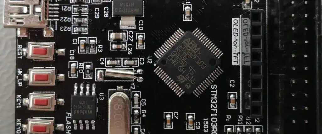
III. Understanding the Blue Pill Board (STM32F103C8T6)
Before diving into custom STM32 PCB design, it’s essential to understand the Blue Pill board, which serves as an excellent starting point for many projects.
Pinout and Core Components
The Blue Pill board is built around the STM32F103C8T6 microcontroller and includes several key components:
- STM32F103C8T6 MCU:
- 72 MHz ARM Cortex-M3 core
- 64 KB Flash memory, 20 KB SRAM
- Various peripherals (USART, SPI, I2C, USB, CAN, etc.)
- Power Supply:
- 3.3V regulator for the MCU
- 5V input via USB or external source
- Crystal Oscillators:
- 8 MHz main oscillator
- 32.768 kHz RTC oscillator (not populated by default)
- User Interfaces:
- User LED (PC13)
- BOOT0 and RESET buttons
- Programming Interfaces:
- SWD header for debugging
- USB for power and communication
- I/O Headers:
- All MCU pins broken out to headers
Limitations of Off-the-Shelf Boards
While the Blue Pill is an excellent prototyping platform, it has limitations for production use:
- Form Factor:
- Fixed size and shape may not fit all project enclosures
- Component Selection:
- Limited to pre-selected components, which may not be optimal for all applications
- Power Efficiency:
- Generic design may not be optimized for low-power applications
- Peripheral Access:
- Not all MCU features may be easily accessible
- Customization:
- Limited ability to add project-specific components or interfaces
When to Move to a Custom STM32 PCB
Consider designing a custom STM32 PCB when:
- You need a specific form factor or size constraint
- Your project requires additional components or interfaces not present on the Blue Pill
- You aim to optimize power consumption for battery-operated devices
- You want to reduce production costs for medium to large-scale manufacturing
- Your application needs enhanced reliability or specific certifications
- You’re developing a commercial product and need full control over the design
Moving to a custom STM32 PCB allows you to tailor the design to your specific needs, optimize performance, and potentially reduce costs in production scenarios.
IV. Step 1: Define Your STM32 Project Requirements

Before embarking on your STM32 PCB design journey, it’s crucial to clearly define your project requirements. This step will guide your decisions throughout the design process and help ensure your final PCB meets all necessary specifications.
Choosing the Right STM32 MCU Variant
While this guide focuses on the STM32F103C8T6, there are numerous STM32 variants to choose from:
- Performance requirements:
- Clock speed (from 48 MHz to 480 MHz)
- Memory size (Flash and RAM)
- FPU (Floating Point Unit) presence
- Peripherals needed:
- Number and type of communication interfaces
- ADC resolution and sampling rate
- Timer functionality
- Power consumption:
- Low-power modes available
- Sleep current
- Package type and size:
- LQFP, BGA, or other package options
- Pin count (from 32 to 200+ pins)
Use STM32CubeMX or ST’s product selector tool to find the best match for your project.
Peripheral Needs
List all the peripherals your project requires:
- Communication interfaces:
- UART for serial communication
- I2C for sensor integration
- SPI for high-speed data transfer
- USB for PC connectivity or power
- CAN for industrial applications
- Analog interfaces:
- ADC for sensor readings
- DAC for signal generation
- Timing and control:
- PWM for motor control or LED dimming
- General-purpose timers
- External memory interface:
- FSMC for connecting external RAM or Flash
- Debug interface:
- SWD for programming and debugging
Power Supply and Voltage Regulation
Consider your power supply requirements:
- Input voltage range:
- Battery-powered or mains-powered?
- USB power option?
- Voltage regulation:
- Linear regulators for low noise
- Switching regulators for high efficiency
- Multiple voltage domains:
- 3.3V for the MCU core
- 5V or 12V for peripheral components
- Power consumption:
- Estimated current draw
- Need for low-power modes
Size, Enclosure, and I/O Considerations
Factor in physical constraints:
- PCB dimensions:
- Maximum size allowed by the enclosure
- Multi-board design for complex systems
- Enclosure requirements:
- Environmental protection (IP rating)
- Heat dissipation needs
- I/O access:
- Connectors for external interfaces
- Test points for debugging
- User interface elements:
- LEDs for status indication
- Buttons or switches for user input
- Mounting considerations:
- Screw holes or standoffs
- Edge connectors for modular designs
By thoroughly defining these requirements, you set a solid foundation for your STM32 PCB design, ensuring that the final product will meet all necessary specifications and perform optimally in its intended application.
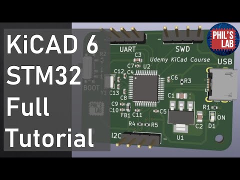
V. Step 2: STM32 Schematic Design
With your project requirements clearly defined, the next step is to create the schematic for your custom STM32 PCB. The schematic is a detailed diagram that represents all the electrical connections in your circuit.
Using EDA Tools
Several Electronic Design Automation (EDA) tools are popular for STM32 PCB design:
- KiCad:
- Open-source and free
- Powerful features and growing community support
- Eagle:
- Popular among hobbyists and small businesses
- Extensive component libraries
- Altium Designer:
- Professional-grade tool with advanced features
- Excellent for complex, multi-layer designs
Choose a tool that matches your skill level and project complexity. Many offer free versions or trials, allowing you to experiment before committing.
Essential Parts of the STM32 Circuit
STM32F103C8T6 Wiring
- Power pins:
- Connect VDD pins to 3.3V
- Connect VSS pins to ground
- Add decoupling capacitors (0.1μF) close to each VDD pin
- Boot mode selection:
- BOOT0 pin with pull-down resistor
- BOOT1 pin (PB2) with pull-down resistor
- Reset circuit:
- NRST pin with pull-up resistor and capacitor to ground
- Optional reset button
- Clock sources:
- HSE: 8 MHz crystal with load capacitors
- LSE: 32.768 kHz crystal for RTC (optional)
Power Supply
- Voltage regulator:
- LDO for 3.3V from 5V input
- Consider adding a 5V regulator if using higher input voltages
- Bypass capacitors:
- 10μF to 100μF electrolytic or tantalum near voltage regulators
- 0.1μF ceramic capacitors near ICs
Reset Circuit
- Reset button:
- Momentary switch between NRST and ground
- Series resistor (470Ω) to limit current
- Power-on reset:
- RC circuit with 10kΩ resistor and 0.1μF capacitor
External Crystal Oscillator
- 8 MHz crystal:
- Connected between OSC_IN (PD0) and OSC_OUT (PD1)
- Two load capacitors (typically 20pF) to ground
- Optional 32.768 kHz crystal for RTC:
- Connected between PC14 and PC15
- Two load capacitors (typically 12pF) to ground
Programming Header
- SWD interface:
- SWDIO (PA13) and SWCLK (PA14) pins
- 2×5 pin header for ST-Link compatibility
- UART bootloader (optional):
- USART1 TX (PA9) and RX (PA10) pins
- Consider adding a USB-to-UART bridge chip
Best Practices in STM32 Schematic Design
- Use clear and consistent naming conventions for components and nets.
- Group related components together for better readability.
- Add detailed notes and comments to explain non-obvious design choices.
- Include test points for important signals to aid in debugging.
- Consider adding protection components like TVS diodes for exposed I/O.
- Use hierarchical sheets for complex designs to improve organization.
- Perform thorough Electrical Rule Checks (ERC) to catch common errors.
By following these guidelines and paying attention to detail in your schematic design, you’ll create a solid foundation for the PCB layout phase of your STM32 project.
VI. Step 3: STM32 PCB Layout Best Practices
Once your schematic is complete and error-free, it’s time to move on to the PCB layout. This stage transforms your circuit diagram into a physical board design, considering factors like component placement, trace routing, and signal integrity.
Component Placement Strategy
Effective component placement is crucial for a successful STM32 PCB design:
- Place the STM32 microcontroller centrally:
- This allows for easier routing to peripherals and connectors.
- Group related components:
- Keep decoupling capacitors close to their respective ICs.
- Place crystal oscillators near the MCU’s oscillator pins.
- Consider thermal management:
- Keep heat-generating components (e.g., voltage regulators) away from sensitive parts.
- Optimize for signal integrity:
- Minimize trace lengths for high-speed signals.
- Keep analog and digital sections separated.
- Plan for assembly and testing:
- Align components in a way that simplifies the manufacturing process.
- Leave space for test points near critical signals.
Power and Ground Plane Layout
Proper power distribution is essential for reliable STM32 PCB operation:
- Use solid ground planes:
- Dedicate at least one layer to a continuous ground plane.
- For multi-layer boards, consider using multiple ground planes.
- Implement star grounding:
- Connect sensitive analog grounds to a single point on the main ground plane.
- Use wide traces or copper pours for power distribution:
- Minimize voltage drop across the board.
- Consider using polygons for main power nets.
- Separate analog and digital power:
- Use separate power planes or traces for analog and digital supplies.
- Connect these at a single point near the power source.
Trace Width, Spacing, and Signal Routing
Follow these guidelines for optimal signal routing:
- Calculate appropriate trace widths:
- Use wider traces for power and high-current signals.
- Standard signal traces can be 6-10 mil wide.
- Maintain consistent trace spacing:
- Typically 6-10 mil for standard signals.
- Increase spacing for high-voltage or noisy signals.
- Use 45-degree angles for trace corners:
- Avoid 90-degree bends to reduce reflections.
- Keep high-speed traces short and direct:
- Minimize length and avoid unnecessary vias for critical signals.
- Use differential pair routing for high-speed interfaces:
- Maintain equal length and consistent spacing between pairs.
Guidelines for USB, ADC, and High-Speed I/O Traces
- USB routing:
- Keep D+ and D- traces close and matched in length.
- Maintain 90Ω differential impedance.
- Avoid vias if possible; if necessary, use them in pairs.
- ADC considerations:
- Keep analog traces short and away from digital signals.
- Use a ground guard ring around sensitive analog components.
- Consider using a split ground plane for analog and digital sections.
- High-speed I/O:
- Route clock lines first, then other high-speed signals.
- Use length matching for parallel buses.
- Consider using microstrip or stripline techniques for controlled impedance.
EMI/EMC Considerations in STM32 PCB Layout
- Keep loop areas small for high-frequency signals.
- Use ground planes to provide low-impedance return paths.
- Consider adding ferrite beads on power lines to suppress high-frequency noise.
- Use shielding techniques for sensitive analog circuits or in noisy environments.
- Implement proper grounding for connectors and I/O ports.
Two-Layer vs. Four-Layer Design Decisions
When designing your STM32 PCB, you’ll need to choose between a two-layer or four-layer board:
Two-Layer PCBs:
- Pros: Lower cost, simpler manufacturing process.
- Cons: More challenging routing, potential signal integrity issues.
- Best for: Simple designs, low-speed applications, cost-sensitive projects.
Four-Layer PCBs:
- Pros: Better signal integrity, easier routing, dedicated power/ground planes.
- Cons: Higher cost, more complex manufacturing.
- Best for: Complex designs, high-speed signals, professional products.
For most STM32 projects, a four-layer board offers the best balance of performance and design flexibility. A typical four-layer stackup might include:
- Top layer: Components and signal routing
- Inner layer 1: Ground plane
- Inner layer 2: Power plane
- Bottom layer: Components and signal routing
This configuration provides excellent signal integrity and simplifies power distribution.
VII. Step 4: Prototyping and Fabrication
After completing your PCB layout, the next exciting phase is bringing your design to life through prototyping and fabrication.
Generating Gerber Files and BOM
- Gerber file generation:
- Use your EDA tool to export Gerber files, which contain all the necessary information for PCB fabrication.
- Include files for all copper layers, solder mask, silkscreen, and drill holes.
- Double-check that all layers are correctly aligned and scaled.
- Creating a Bill of Materials (BOM):
- List all components, including their values, packages, and quantities.
- Include manufacturer part numbers and potential alternative parts.
- Organize the BOM in a clear, spreadsheet format for easy reference.
PCB Prototyping Services
For prototype runs or small batches, consider these popular PCB fabrication services:
- JLCPCB:
- Known for fast turnaround and low costs.
- Offers PCB assembly services as well.
- PCBWay:
- Wide range of PCB manufacturing options.
- Good for both prototypes and small production runs.
- OSH Park:
- Specializes in high-quality, small-batch PCBs.
- Purple solder mask is their signature look.
When selecting a service, consider:
- Minimum order quantity
- Turnaround time
- Board specifications (layer count, minimum trace width, etc.)
- Quality and reliability
- Additional services like stencil manufacturing or assembly
Assembly: Manual Soldering vs. Reflow Oven
Decide between manual soldering and reflow soldering based on your design complexity and component types:
Manual Soldering:
- Suitable for through-hole components and simple designs.
- Requires patience and steady hands.
- Use a temperature-controlled soldering iron and appropriate flux.
Reflow Soldering:
- Better for designs with many surface-mount components.
- Requires a reflow oven or hot air station.
- Steps include:
- Applying solder paste using a stencil
- Placing components with tweezers or a pick-and-place machine
- Carefully controlling temperature profile in the reflow oven
For many STM32 projects, a combination of both methods might be necessary.
Testing the Custom STM32 Board
Once assembled, it’s crucial to thoroughly test your custom STM32 PCB:
- Visual inspection:
- Check for solder bridges, missing components, or obvious defects.
- Continuity testing:
- Use a multimeter to verify connections and check for shorts.
- Power-up test:
- Use a current-limited power supply for initial power-up.
- Monitor power consumption and check voltage levels at key points.
- Functional testing:
- Upload a simple test firmware (e.g., blinking LED).
- Verify basic functionality of all major subsystems.
- Comprehensive testing:
- Test all peripherals and interfaces.
- Perform stress tests under various operating conditions.
VIII. Step 5: Programming and Debugging STM32 PCBs
With your custom STM32 PCB assembled and basic functionality verified, it’s time to dive into programming and debugging your board.
Uploading Firmware to STM32
There are two primary methods for uploading firmware to your STM32 board:
1. SWD with ST-Link V2
Serial Wire Debug (SWD) is the most common method for programming and debugging STM32 microcontrollers:
- Connect ST-Link V2 programmer to your board’s SWD header.
- Use STM32CubeIDE or OpenOCD to upload firmware.
- Allows for real-time debugging and breakpoints.
2. UART Bootloader with USB-to-Serial Adapter
For boards without an SWD header or for field updates:
- Activate bootloader mode (usually by setting BOOT0 pin high).
- Connect a USB-to-Serial adapter to the UART pins.
- Use STM32CubeProgrammer or other flashing tools to upload firmware.
Tools for STM32 Development
- STM32CubeIDE:
- Integrated Development Environment for STM32 programming.
- Includes debugging capabilities and peripheral configuration tools.
- STM32CubeMX:
- Graphical tool for STM32 microcontroller configuration.
- Generates initialization code based on your configuration.
- OpenOCD:
- Open-source debugging tool, useful for command-line enthusiasts.
- Can be integrated with GDB for advanced debugging.
Basic Firmware Setup for Testing I/O
To verify your custom STM32 PCB’s functionality, start with a simple firmware test:
- LED blink test:
- Configure a GPIO pin as output.
- Toggle the pin state in a loop with a delay.
- Button input test:
- Configure a GPIO pin as input with pull-up.
- Read the pin state and toggle an LED based on button press.
- UART communication test:
- Initialize UART peripheral.
- Implement a simple echo program or periodic message transmission.
These basic tests help verify core functionality before moving on to more complex applications.
IX. Design Tips for Reliable STM32 PCBs
To ensure your custom STM32 PCB performs reliably in real-world conditions, consider these advanced design tips:
Decoupling Capacitor Placement
Proper decoupling is crucial for stable operation:
- Place 0.1μF ceramic capacitors as close as possible to each VDD pin.
- Use larger capacitors (1-10μF) near voltage regulators.
- Consider using ferrite beads in series with power lines for additional filtering.
Reset and Boot Mode Management
Ensure reliable startup and programming:
- Implement proper reset circuitry with a pull-up resistor and capacitor.
- Use jumpers or DIP switches for BOOT0/BOOT1 selection if needed.
- Consider adding an external watchdog timer for enhanced reliability.
Over-Voltage and ESD Protection
Protect your STM32 from electrical hazards:
- Use TVS diodes on exposed I/O pins.
- Implement reverse polarity protection on power inputs.
- Consider adding ESD protection devices on communication interfaces.
Design for Manufacturability and Testability
Optimize your design for production and quality assurance:
- Use standard component sizes and packages when possible.
- Include test points for critical signals.
- Consider adding a PCB version number and date code.
- Design for automated optical inspection (AOI) by ensuring adequate clearance around components.
X. Real-World Applications of STM32 Custom Boards
Custom STM32 PCBs find applications in various fields:
Wearables
- Fitness trackers with integrated sensors
- Smart watches with custom displays
- Health monitoring devices
Smart Sensors
- IoT-enabled environmental monitors
- Industrial process control sensors
- Smart home automation devices
Drones and Robotics
- Flight controllers for quadcopters
- Motor control boards for robotic arms
- Navigation systems for autonomous vehicles
DIY and Maker Projects
- Custom game consoles
- Audio processing devices
- Open-source scientific instruments
These examples demonstrate the versatility of STM32 microcontrollers and the potential of custom PCB designs in bringing innovative ideas to life.
XI. Resources and Tools
To further your STM32 PCB design skills, explore these resources:
STM32CubeMX and STM32CubeIDE
- Official ST tools for STM32 configuration and development
- Extensive documentation and tutorials available on ST’s website
Reference Schematics and PCB Layouts
- ST’s Nucleo and Discovery board designs
- Open-source projects on platforms like GitHub
STM32 Datasheets and Application Notes
- Detailed technical information on STM32 microcontrollers
- Best practices and design guidelines from ST
Online Communities and Forums
- STM32Duino: Community-driven Arduino-like environment for STM32
- ST Community: Official forum for STM32 developers
- Reddit r/embedded: Discussions on embedded systems, including STM32
XII. Conclusion
The journey from the Blue Pill to a fully customized STM32 PCB is both challenging and rewarding. By mastering the art of STM32 PCB design, you open the door to creating highly optimized, application-specific embedded systems.
Whether you’re upgrading from the Blue Pill or building a product, mastering STM32 PCB design opens the door to professional embedded development. The skills you’ve gained in schematic design, PCB layout, and prototyping are invaluable in today’s technology-driven world.
Remember that PCB design is both an art and a science. While following best practices is important, there’s also room for creativity and innovation. Each project brings new challenges and opportunities for learning.
We encourage you to start designing your own STM32 boards. Begin with simple designs, gradually tackling more complex challenges. Experiment with different peripherals, explore various STM32 variants, and push the boundaries of what’s possible within the constraints of PCB design.
The field of embedded systems is ever-evolving, with STM32 at the forefront of many innovations. Stay curious, keep learning, and don’t hesitate to engage with the vibrant community of makers, engineers, and hobbyists who share your passion for STM32 PCB design.
Your next custom STM32 PCB could be the foundation of a groundbreaking product or the solution to a complex problem. So fire up your favorite EDA tool, choose an STM32 microcontroller, and start designing. The world of custom STM32 PCBs awaits your creativity and expertise!
XIII. FAQ
To address common queries and enhance SEO, here are answers to frequently asked questions about STM32 PCB design:
What is the STM32F103C8T6 Blue Pill?
The STM32F103C8T6 Blue Pill is a popular, low-cost development board featuring the STM32F103C8T6 microcontroller. It’s known for its compact size, breadboard-friendly design, and extensive GPIO options, making it a favorite among hobbyists and prototypers for STM32-based projects.
How do I design a custom STM32 PCB?
Designing a custom STM32 PCB involves several steps:
- Define your project requirements and choose an appropriate STM32 microcontroller.
- Create a schematic diagram using EDA software.
- Develop the PCB layout, carefully placing components and routing traces.
- Generate manufacturing files (Gerbers) and order a prototype.
- Assemble and test your PCB, making iterations as necessary.
Which software is best for STM32 PCB layout?
Popular software options for STM32 PCB layout include:
- KiCad: Free, open-source, and feature-rich.
- Altium Designer: Professional-grade with advanced features.
- Eagle: User-friendly with a large component library.
- Fusion 360 Electronics: Integrates electrical and mechanical design.
Choose software that aligns with your project complexity and budget.
Can I use STM32CubeMX for PCB design?
STM32CubeMX is primarily a microcontroller configuration and code generation tool, not a PCB design software. However, it can be extremely useful in the early stages of PCB design:
- It helps in pin assignment and peripheral configuration.
- It can generate a partial schematic of the microcontroller connections.
- The configuration can be exported to PCB design tools for further development.
For actual PCB layout, you’ll need to use dedicated EDA software.
How do I program a custom STM32 board?
Programming a custom STM32 board can be done in several ways:
- Using SWD (Serial Wire Debug) with an ST-Link programmer:
- Connect the ST-Link to your board’s SWD pins.
- Use STM32CubeIDE or OpenOCD to upload firmware.
- Using the UART bootloader:
- Set the BOOT0 pin high to enter bootloader mode.
- Use a USB-to-UART adapter and STM32CubeProgrammer to upload firmware.
- Using a custom bootloader:
- Implement a bootloader that allows firmware updates over various interfaces (USB, CAN, Ethernet, etc.).
The method you choose depends on your board design and project requirements.