In the intricate world of Printed Circuit Board (PCB) design and manufacturing, every detail matters. One crucial aspect that often doesn’t receive the attention it deserves is solder mask expansion. This article delves deep into the concept of solder mask expansion, its importance in PCB design, and how to implement it effectively. Whether you’re a novice PCB designer or a seasoned professional, understanding solder mask expansion is key to creating high-quality, reliable circuit boards.
What is Solder Mask Expansion?
Before we dive into the intricacies of solder mask expansion, it’s essential to understand what it is and why it’s so important in PCB design.
Definition of Solder Mask Expansion
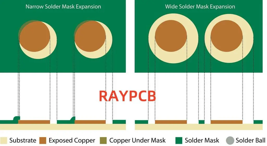
Solder mask expansion refers to the distance by which the solder mask opening is larger than the copper pad or via on a PCB. It’s a critical parameter that affects the quality of solder joints, the reliability of connections, and the overall manufacturability of the board.
The Importance of Solder Mask Expansion
Proper solder mask expansion serves several crucial functions:
- Improved Solderability: It ensures that there’s enough exposed copper for the solder to adhere to, creating strong and reliable connections.
- Prevention of Solder Bridging: By controlling the flow of solder during the assembly process, it helps prevent unwanted connections between adjacent pads.
- Protection Against Oxidation: It shields the copper traces from environmental factors that could lead to oxidation and degradation over time.
- Enhanced Visual Inspection: A well-designed solder mask expansion makes it easier to visually inspect solder joints for quality control purposes.
Types of Solder Mask Expansion
There are two main types of solder mask expansion:
- Positive Expansion: The solder mask opening is larger than the copper pad or via. This is the most common type and is used in most applications.
- Negative Expansion: The solder mask opening is smaller than the copper pad or via. This is less common and is used in specific situations, such as with certain BGA (Ball Grid Array) components.
Key Settings for Solder Mask Expansion
Achieving the right solder mask expansion involves careful consideration of several key parameters. Let’s explore these in detail.
Solder Mask Expansion Value
The solder mask expansion value is typically expressed in mils (thousandths of an inch) or micrometers. Common values include:
- For through-hole components: 2-3 mils (50-75 μm)
- For surface mount components: 1-2 mils (25-50 μm)
Solder Mask Clearance
Solder mask clearance refers to the minimum distance between the edge of the copper pad and the edge of the solder mask opening. Typical clearance values are:
- Minimum clearance: 2 mils (50 μm)
- Recommended clearance: 3-4 mils (75-100 μm)
Solder Mask Dam
The solder mask dam is the area of solder mask between two adjacent pads. Maintaining an adequate dam width is crucial for preventing solder bridges. Recommended dam widths are:
- Minimum dam width: 4 mils (100 μm)
- Recommended dam width: 6-8 mils (150-200 μm)
Read more about:
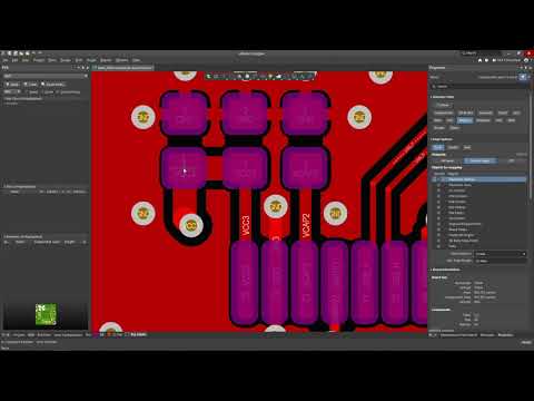
How to Design Solder Mask Expansion in Altium
Altium Designer is a popular PCB design software that offers powerful tools for managing solder mask expansion. Here’s a step-by-step guide to setting up solder mask expansion in Altium:
1. Accessing Solder Mask Expansion Settings
- Open your PCB project in Altium Designer.
- Go to “Design” > “Rules” to open the PCB Rules and Constraints Editor.
- Expand the “Manufacturing” category in the left panel.
- Select “Solder Mask Expansion” under the “Mask” subcategory.
2. Configuring Global Solder Mask Expansion Rules
- In the “Solder Mask Expansion” window, click “Add Rule”.
- Set a name for your rule (e.g., “Global Solder Mask Expansion”).
- In the “Where The Object Matches” section, set it to “All”.
- In the “Constraints” section, set your desired expansion value.
3. Creating Component-Specific Rules
- Follow steps 1-2 from the previous section.
- In the “Where The Object Matches” section, use the query helper to define specific components or areas of the board.
- Set the constraints for these specific components or areas.
4. Verifying Solder Mask Expansion
- Use the “Design Rule Check” (DRC) feature to verify your solder mask expansion settings.
- Go to “Tools” > “Design Rule Check”.
- Ensure that the “Mask” rules are selected in the DRC dialog.
- Run the DRC and review any violations related to solder mask expansion.
5. Visualizing Solder Mask Expansion
- In the PCB editor, go to the “View” menu.
- Enable the “Solder Mask” layer to visualize the solder mask openings.
- Use the measurement tools to verify the expansion values manually if needed.
Best Practices for Solder Mask Expansion

Implementing solder mask expansion effectively requires adherence to several best practices. Here are some key guidelines to follow:
1. Consistency is Key
Maintain consistent solder mask expansion values across similar components on your PCB. This ensures uniform soldering results and simplifies the manufacturing process.
2. Consider Component Types
Different component types may require different expansion values:
- Through-hole components typically need larger expansions than surface mount components.
- Fine-pitch components may require smaller expansions to prevent solder bridging.
3. Account for Manufacturing Tolerances
Always consider the manufacturing tolerances of your PCB fabricator when setting solder mask expansion values. It’s often wise to add a small buffer to account for these tolerances.
4. Balance Between Expansion and Dam Width
Ensure that your solder mask expansion doesn’t compromise the dam width between adjacent pads. This is particularly important for fine-pitch components.
5. Use Teardrop Pads Wisely
For vias and through-hole pads, consider using teardrop pads with appropriate solder mask expansion to improve mechanical strength and solderability.
6. Verify with Your Manufacturer
Always consult with your PCB manufacturer to ensure your solder mask expansion settings align with their capabilities and recommendations.
Common Mistakes & Troubleshooting

Even experienced PCB designers can sometimes fall into pitfalls when it comes to solder mask expansion. Here are some common mistakes and how to troubleshoot them:
1. Too Little Expansion
Problem: Insufficient solder mask expansion can lead to poor solder joints and increased risk of oxidation.
Symptoms:
- Weak or unreliable solder connections
- Visible copper around the edges of solder joints
Solution:
- Increase the solder mask expansion value
- Ensure the expansion is at least 1-2 mils (25-50 μm) for most applications
2. Too Much Expansion
Problem: Excessive solder mask expansion can cause solder bridging and component misalignment.
Symptoms:
- Solder bridges between adjacent pads
- Components shifting during the soldering process
Solution:
- Reduce the solder mask expansion value
- Maintain adequate dam width between pads
- Consider using solder mask defined (SMD) pads for fine-pitch components
3. Misalignment Issues
Problem: Misalignment between the solder mask layer and the copper layer can lead to partially covered pads.
Symptoms:
- Inconsistent solder joints
- Difficulty in visual inspection
Solution:
- Verify the alignment of all layers in your PCB design software
- Use fiducial markers to improve layer alignment during manufacturing
- Consider increasing the solder mask expansion slightly to account for minor misalignments
4. Inconsistent Expansion Values
Problem: Using different expansion values for similar components can lead to inconsistent soldering results.
Symptoms:
- Varying solder joint quality across the board
- Difficulty in automated assembly processes
Solution:
- Review and standardize solder mask expansion rules in your design software
- Create component-specific rules for different types of parts
- Document your expansion standards for future reference
5. Ignoring Via Treatment
Problem: Failing to properly handle vias in solder mask design can lead to solder wicking and unreliable connections.
Symptoms:
- Solder flowing through vias during assembly
- Weak or inconsistent via connections
Solution:
- Use tented vias (covered by solder mask) for small vias not used for component connections
- For exposed vias, ensure proper solder mask expansion to prevent excessive solder flow
- Consider via plugging for critical applications
Advanced Considerations
As PCB designs become more complex, there are several advanced considerations to keep in mind when it comes to solder mask expansion:
1. High-Frequency Applications
In high-frequency PCB designs, solder mask expansion can impact signal integrity:
- Consider selective removal of solder mask in critical RF areas
- Use controlled impedance calculations to determine optimal solder mask expansion
2. Flex and Rigid-Flex PCBs
Flexible and rigid-flex PCBs present unique challenges:
- Use flexible solder mask materials that can withstand bending
- Consider larger solder mask expansions to account for material movement
3. Fine-Pitch and BGA Components
For extremely fine-pitch components and BGAs:
- Use solder mask defined (SMD) pads to control solder paste volume
- Consider laser-defined solder mask openings for highest precision
4. Thermal Management
In designs with high thermal stress:
- Use selective solder mask expansion to create thermal relief patterns
- Consider the impact of solder mask on heat dissipation in power components
5. Automated Optical Inspection (AOI)
To facilitate AOI processes:
- Ensure consistent solder mask expansion for similar component types
- Consider the contrast between solder mask color and pad finish
Conclusion: Mastering Solder Mask Expansion
Solder mask expansion is a critical aspect of PCB design that impacts the quality, reliability, and manufacturability of your boards. By understanding the principles behind solder mask expansion, following best practices, and avoiding common pitfalls, you can significantly improve the performance of your PCBs.
Remember that while guidelines are helpful, every PCB design is unique. Always consider the specific requirements of your project, consult with your manufacturer, and be willing to iterate on your design to achieve optimal results.
Mastering solder mask expansion is an ongoing process that combines theoretical knowledge with practical experience. As you continue to design and manufacture PCBs, you’ll develop an intuitive understanding of how to balance the various factors involved in solder mask expansion.
By paying attention to this often-overlooked aspect of PCB design, you’ll be well on your way to creating high-quality, reliable circuit boards that meet the demanding requirements of modern electronic devices.