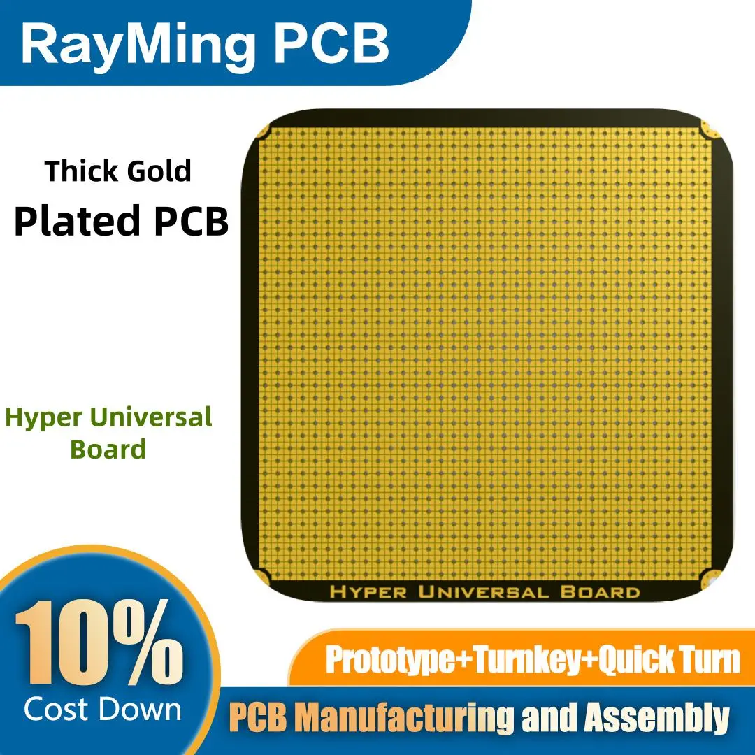
The Hyper Universal Board with thick gold plated PCB is an advanced electronic component designed for high-performance and versatile applications. This specialized board features a substantially thicker layer of gold plating compared to standard PCBs, offering superior conductivity, durability, and reliability.
The thick gold plating, typically ranging from 30 to 50 microinches or more, provides exceptional protection against corrosion and oxidation. This makes it ideal for harsh environments or applications requiring long-term stability. The increased thickness also enhances the board’s ability to withstand multiple insertion cycles, making it suitable for applications that require frequent connections or testing.
The “universal” aspect of the board refers to its adaptability to various electronic designs and components. It often includes a range of pre-drilled holes, pads, and traces that can accommodate different circuit configurations, allowing for rapid prototyping and flexible design implementations.
The combination of thick gold plating and universal design makes this board particularly valuable in industries such as aerospace, medical devices, telecommunications, and high-end consumer electronics. It offers engineers and designers a robust platform for developing complex, high-reliability circuits without compromising on performance or longevity.
Moreover, the Hyper Universal Board’s thick gold plating ensures excellent signal integrity, minimal signal loss, and reduced electromagnetic interference, crucial for high-frequency applications and sensitive analog circuits.