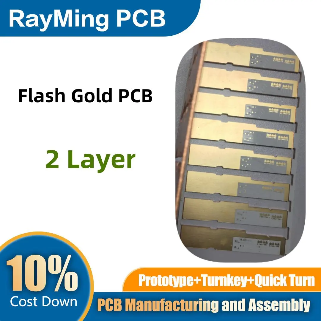
2 Layer flash gold PCB refers to a printed circuit board with two conductive layers and a specific surface finish known as flash gold. This finish involves depositing an extremely thin layer of gold onto the copper surfaces of the PCB, typically less than 1 microinch (0.025 micrometers) thick.
Flash gold, also called “soft gold” or “electrolytic gold flash,” is applied through an electrolytic process. It provides several benefits:
- Improved solderability: The gold layer protects the copper from oxidation, ensuring better solder joint quality.
- Enhanced contact reliability: Ideal for edge connectors and contact fingers.
- Cost-effectiveness: Uses less gold than thicker finishes like ENIG, reducing overall costs.
- Compatibility: Suitable for both lead and lead-free soldering processes.
However, flash gold has limitations:
- Short shelf life: The thin layer offers limited protection against copper oxidation over time.
- Not suitable for wire bonding: The gold layer is too thin for this application.
- Potential for porosity: The ultra-thin layer may have microscopic pores, potentially exposing the underlying copper.
2 Layer flash gold PCBs are commonly used in consumer electronics, automotive applications, and other products where cost-effectiveness and good solderability are priorities, but extended shelf life isn’t critical.