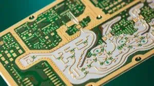
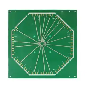
In the rapidly evolving world of electronics, radio frequency (RF) circuits play a crucial role in wireless communication systems, radar technology, and numerous other applications. Designing printed circuit boards (PCBs) for RF circuits presents unique challenges, particularly in ensuring electromagnetic compatibility (EMC). This article delves into the intricacies of PCB design for RF circuits, focusing on key principles, best practices, and strategies to achieve optimal performance while maintaining electromagnetic compatibility.

Understanding RF Circuits and Electromagnetic Compatibility
What are RF Circuits?
Radio Frequency circuits operate in the frequency range from about 3 kHz to 300 GHz. These circuits are essential in various applications, including:
- Wireless communication devices
- Radar systems
- Satellite communications
- Broadcasting equipment
- Medical imaging devices
The Importance of Electromagnetic Compatibility
Electromagnetic Compatibility (EMC) refers to the ability of electronic equipment to function correctly in its intended electromagnetic environment without introducing intolerable electromagnetic disturbances to other equipment. In RF circuit design, EMC is crucial for:
- Ensuring proper functionality of the circuit
- Complying with regulatory standards
- Minimizing interference with other devices
- Enhancing overall system reliability
Key Considerations in RF PCB Design
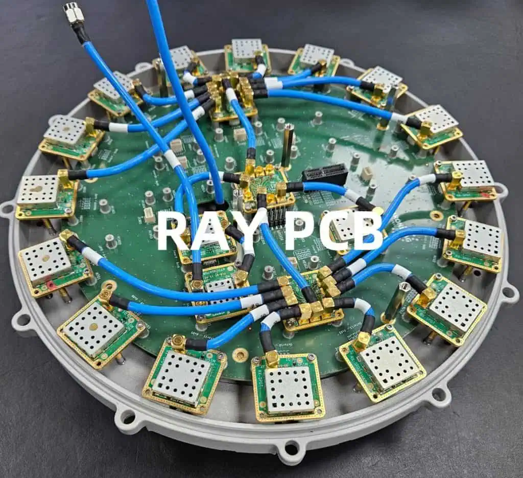
1. Substrate Selection
The choice of PCB substrate is critical in RF design due to its impact on signal propagation and loss.
Factors to consider:
- Dielectric constant (εr)
- Loss tangent (tan δ)
- Thickness
- Thermal stability
- Cost
Comparison of common RF PCB substrates:
| Substrate Material | Dielectric Constant (εr) | Loss Tangent (tan δ) | Thermal Stability | Relative Cost |
| FR-4 | 4.2-4.8 | 0.02 | Moderate | Low |
| Rogers RO4350B | 3.48 | 0.0037 | Excellent | Moderate |
| Taconic RF-35 | 3.5 | 0.0018 | Good | Moderate |
| PTFE (Teflon) | 2.1 | 0.0002 | Excellent | High |
2. Impedance Matching and Control
Maintaining consistent impedance throughout the RF signal path is crucial for minimizing reflections and maximizing power transfer.
Key aspects:
- Transmission line width calculation
- Use of impedance calculators
- Consideration of manufacturing tolerances
3. Transmission Line Design
Proper transmission line design is essential for efficient signal propagation in RF circuits.
Common transmission line types:
- Microstrip
- Stripline
- Coplanar waveguide (CPW)
Factors affecting transmission line performance:
- Line width and spacing
- Substrate thickness
- Dielectric constant
- Ground plane proximity
4. Ground Plane Design
A well-designed ground plane is crucial for RF performance and EMC.
Best practices:
- Use of solid ground planes
- Minimizing splits or gaps
- Proper via stitching
- Consideration of return current paths
5. Component Placement and Routing
Strategic placement and routing of components are vital for RF circuit performance.
Guidelines:
- Keep RF traces short and direct
- Use symmetrical layouts for differential pairs
- Avoid right-angle bends in RF traces
- Maintain adequate spacing between RF and digital sections
6. Shielding and Isolation
Effective shielding and isolation techniques help minimize electromagnetic interference (EMI) and crosstalk.
Techniques:
- Use of EMI shields
- Implementation of guard traces
- Proper partitioning of RF and digital sections
- Use of via fencing
Advanced RF PCB Design Techniques
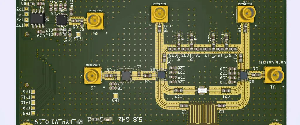
1. Multi-Layer RF PCB Design
Multi-layer PCBs offer additional flexibility and performance benefits for complex RF designs.
Advantages:
- Improved isolation between circuits
- More efficient use of board space
- Enhanced power distribution
- Better control of impedance and crosstalk
Design considerations:
- Layer stack-up optimization
- Proper use of buried and blind vias
- Careful management of interlayer transitions
2. High-Speed Digital Interfaces in RF Designs
Many modern RF systems incorporate high-speed digital interfaces, requiring special design considerations.
Key points:
- Proper termination of high-speed lines
- Controlled impedance routing
- Minimizing crosstalk between digital and RF sections
- Use of appropriate decoupling techniques
3. Thermal Management in RF PCBs
Effective thermal management is crucial for the reliability and performance of RF circuits.
Strategies:
- Use of thermal vias
- Implementation of copper coins or heat sinks
- Proper component placement for heat dissipation
- Consideration of thermal simulation tools
4. Design for Manufacturability and Testability
Ensuring that RF PCBs are manufacturable and testable is essential for successful production.
Considerations:
- Adherence to manufacturing design rules
- Inclusion of test points and probe access
- Consideration of automated assembly requirements
- Documentation of critical RF parameters and tolerances
EMC Considerations in RF PCB Design
1. EMI Reduction Techniques
Minimizing electromagnetic interference is crucial for both circuit performance and regulatory compliance.
Strategies:
- Proper grounding and shielding
- Use of EMI suppression components
- Filtering of power supplies
- Careful routing to minimize EMI coupling
2. EMC Testing and Compliance
Understanding and designing for EMC compliance is essential in RF PCB development.
Key aspects:
- Familiarity with relevant EMC standards (e.g., FCC, CE)
- Design for pre-compliance testing
- Consideration of EMC test setups in PCB design
- Documentation of EMC design choices and rationale
3. Radiated Emissions Control
Controlling radiated emissions is a critical aspect of EMC in RF PCB design.
Techniques:
- Minimizing loop areas in current paths
- Proper termination of unused traces
- Use of spread spectrum techniques where applicable
- Implementation of EMI gaskets and conductive coatings
4. Susceptibility and Immunity Considerations
Ensuring that RF circuits are resistant to external electromagnetic interference is crucial for reliable operation.
Design strategies:
- Proper filtering of input/output lines
- Use of differential signaling where appropriate
- Implementation of guard bands around sensitive circuits
- Consideration of board-level shielding techniques
Tools and Software for RF PCB Design
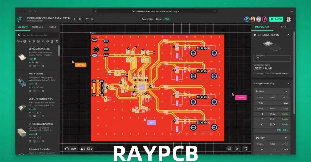
1. Electromagnetic Simulation Tools
EM simulation tools are invaluable for predicting and optimizing RF PCB performance.
Popular tools:
- Ansys HFSS
- CST Microwave Studio
- Keysight ADS
- Sonnet Software
2. PCB Design Software with RF Capabilities
Specialized PCB design software with RF features can greatly aid in the design process.
Key features to look for:
- Impedance-controlled routing
- RF-specific component libraries
- Integration with EM simulation tools
- Advanced stackup management
3. Signal Integrity and Power Integrity Analysis Tools
SI/PI tools help ensure proper signal transmission and power distribution in RF designs.
Important capabilities:
- Time-domain reflectometry (TDR) simulation
- S-parameter analysis
- Power distribution network (PDN) analysis
- Crosstalk prediction and mitigation
Best Practices for RF PCB Design and EMC
1. Design Planning and Documentation
Thorough planning and documentation are crucial for successful RF PCB design.
Key elements:
- Detailed specification of RF performance requirements
- Documentation of EMC considerations and strategies
- Clear definition of critical RF paths and components
- Maintenance of design revision history
2. Prototyping and Iterative Design
Embracing an iterative design approach with prototyping can lead to optimized RF PCB performance.
Best practices:
- Use of evaluation boards for critical components
- Implementation of modular design for easy modification
- Planned iterations for performance optimization
- Thorough testing at each design stage
3. Collaboration between RF, Digital, and PCB Designers
Effective collaboration among different design disciplines is essential for complex RF PCBs.
Strategies for success:
- Regular design reviews and cross-functional meetings
- Clear communication of design constraints and requirements
- Use of collaborative design tools and platforms
- Shared understanding of EMC goals and challenges
4. Continuous Learning and Industry Trends
Staying updated with the latest RF and EMC design techniques is crucial in this rapidly evolving field.
Ways to stay current:
- Attendance at industry conferences and workshops
- Participation in professional organizations (e.g., IEEE)
- Regular review of technical literature and standards
- Engagement with component manufacturers and tool vendors
Future Trends in RF PCB Design and EMC
1. 5G and Beyond
The rollout of 5G and development of future wireless technologies will drive innovations in RF PCB design.
Emerging challenges:
- Design for millimeter-wave frequencies
- Integration of massive MIMO systems
- Balancing performance and power efficiency
- Addressing new EMC challenges at higher frequencies
2. Internet of Things (IoT) and Wearable Devices
The proliferation of IoT and wearable devices presents unique RF and EMC design challenges.
Key considerations:
- Miniaturization of RF circuits
- Design for ultra-low power consumption
- EMC in densely populated IoT environments
- Integration of multiple wireless standards in single devices
3. Advanced Materials and Manufacturing Techniques
New materials and manufacturing methods are expanding the possibilities in RF PCB design.
Emerging trends:
- Use of engineered substrates for enhanced RF performance
- 3D-printed RF components and structures
- Integration of RF-MEMS devices
- Flexible and stretchable RF circuits
4. Artificial Intelligence in RF PCB Design
AI and machine learning are beginning to play a role in optimizing RF PCB designs.
Potential applications:
- Automated optimization of component placement and routing
- Predictive modeling of EMC performance
- AI-assisted design rule checking for RF circuits
- Machine learning for rapid prototyping and design iteration
Conclusion
Designing PCBs for radio frequency circuits while ensuring electromagnetic compatibility is a complex and challenging task that requires a deep understanding of RF principles, EMC considerations, and PCB design techniques. By following best practices, leveraging appropriate tools, and staying abreast of emerging trends, engineers can create RF PCBs that meet stringent performance requirements while complying with EMC standards.
As the demand for wireless communication and RF-enabled devices continues to grow, the importance of skilled RF PCB design will only increase. The field will continue to evolve, driven by advancements in technology, materials, and design methodologies. Engineers who can effectively navigate the intricate balance between RF performance and electromagnetic compatibility will be well-positioned to contribute to the next generation of wireless and RF-enabled systems.
Frequently Asked Questions (FAQ)
1. What are the main differences between designing PCBs for RF circuits and standard digital circuits?
The main differences include:
- Impedance control: RF designs require precise control of trace impedances throughout the signal path.
- Substrate selection: RF circuits often need specialized low-loss substrates.
- Signal integrity: RF designs are more sensitive to issues like reflections and crosstalk.
- EMI/EMC considerations: RF circuits require more stringent EMI/EMC design practices.
- Component selection: RF designs often use specialized components like distributed elements.
2. How does the choice of PCB substrate affect RF performance?
The PCB substrate affects RF performance in several ways:
- Dielectric constant (εr) influences signal propagation speed and wavelength.
- Loss tangent (tan δ) affects signal attenuation and overall circuit efficiency.
- Substrate thickness impacts impedance control and coupling between layers.
- Thermal stability of the substrate affects the circuit’s frequency stability over temperature.
Choosing the right substrate involves balancing these factors along with cost and manufacturability considerations.
3. What are some common EMC issues in RF PCB design, and how can they be mitigated?
Common EMC issues in RF PCB design include:
- Radiated emissions: Mitigated by proper shielding, minimizing loop areas, and controlled impedance routing.
- Conducted emissions: Addressed through proper filtering of power supplies and I/O lines.
- Susceptibility to external interference: Mitigated by proper grounding, filtering, and sometimes board-level shielding.
- Crosstalk between RF and digital sections: Minimized by proper partitioning, use of guard traces, and via fencing.
Mitigation strategies often involve a combination of layout techniques, component selection, and system-level design considerations.
4. How does multi-layer PCB design benefit RF circuits?
Multi-layer PCB design offers several benefits for RF circuits:
- Improved isolation between different circuit sections.
- More efficient use of board space, allowing for more compact designs.
- Better control of impedances and return current paths.
- Ability to implement complex routing schemes like stripline.
- Enhanced power distribution with dedicated power and ground planes.
- Flexibility in implementing different transmission line types within the same board.
However, multi-layer designs also introduce challenges like managing layer transitions and controlling impedance across layers.
5. What are some emerging trends in RF PCB design that engineers should be aware of?
Key emerging trends in RF PCB design include:
- Design for higher frequencies (mmWave) in 5G and beyond applications.
- Integration of multiple wireless standards in single devices for IoT applications.
- Use of advanced materials like liquid crystal polymers (LCP) for improved RF performance.
- Implementation of 3D-printed RF structures for customized solutions.
- Application of AI and machine learning for design optimization and EMC prediction.
- Increased focus on flexible and wearable RF circuits.
- Growing importance of thermal management in high-power RF designs.
Staying informed about these trends helps engineers prepare for future challenges and opportunities in RF PCB design.


