Surface Mount Technology (SMT) has revolutionized the electronics manufacturing industry, enabling the production of smaller, more complex, and highly efficient printed circuit boards (PCBs). A critical aspect of the SMT process is the use of panelized PCBs, which allows for more efficient handling and prototype assembly of multiple boards simultaneously. This article delves into the essential panel requirements for assembly during SMT, exploring the various factors that influence panel design, manufacturing, and processing.
Understanding Panelization in SMT
What is Panelization?
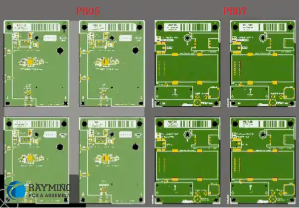
Panelization is the process of combining multiple individual PCBs into a single, larger panel for more efficient production. This approach offers several advantages in SMT assembly:
- Improved handling and automation
- Increased production efficiency
- Better use of manufacturing equipment
- Enhanced quality control
- Reduced material waste
Types of Panels
There are several types of panels used in SMT assembly:
- Array panels: Multiple identical PCBs arranged in a grid
- Mixed panels: Different PCB designs combined on a single panel
- Multiblock panels: Large PCBs segmented into smaller blocks for assembly
- Single PCB panels: Individual PCBs with added borders for handling
Key Panel Requirements for SMT Assembly

1. Panel Size and Thickness
The dimensions and thickness of the panel are crucial for compatibility with SMT equipment and processes.
Factors influencing panel size:
- SMT equipment specifications
- Pick-and-place machine capabilities
- Reflow oven dimensions
- Handling and storage considerations
Standard panel sizes:
| Panel Type | Dimensions (inches) | Typical Applications |
| Full | 18 x 24 | High-volume production |
| Half | 18 x 12 | Medium-volume production |
| Quarter | 12 x 9 | Low-volume or prototype runs |
| Custom | Varies | Specific product requirements |
Panel thickness considerations:
- Typical range: 0.031″ to 0.093″ (0.8mm to 2.4mm)
- Thicker panels may require special handling equipment
- Thinner panels may need additional support to prevent warping
2. Panel Material and Construction
The choice of panel material affects both the manufacturing process and the final product quality.
Common panel materials:
- FR-4 (Flame Retardant 4)
- High-Tg FR-4
- Polyimide
- Ceramic
- Metal-core PCBs
Material selection factors:
- Thermal properties
- Electrical requirements
- Mechanical strength
- Cost considerations
3. Fiducial Marks
Fiducial marks are essential for accurate component placement during SMT assembly.
Types of fiducials:
- Global fiducials (panel-level)
- Local fiducials (board-level)
- Tooling fiducials
Fiducial design guidelines:
- Minimum size: 1mm diameter
- Clearance around fiducial: 2-3mm
- Contrasting color to the PCB surface
- Typically copper with solder mask clearance
4. Tooling Holes and Edges
Proper tooling features ensure accurate alignment and secure handling during the SMT process.
Tooling hole requirements:
- Diameter: Typically 3mm to 4mm
- Location: At least three holes, ideally at corners
- Edge clearance: Minimum 5mm from panel edge
Edge considerations:
- Smooth edges to prevent snagging
- Rounded corners to reduce stress concentration
- Clearance from components and traces
5. Break-out Methods
The method used to separate individual PCBs from the panel affects both manufacturing efficiency and board quality.
Common break-out methods:
- V-scoring
- Perforated tabs
- Route and retain
- Pinned breakaway
Comparison of break-out methods:
| Method | Advantages | Disadvantages |
| V-scoring | Clean break, fast separation | Limited to straight lines, potential for damage |
| Perforated tabs | Flexible design, easy manual separation | Requires finishing, potential for uneven edges |
| Route and retain | Smooth edges, complex shapes possible | More expensive, slower process |
| Pinned breakaway | Strong panel integrity, good for odd shapes | Requires manual separation, potent |
6. Component Clearance and Spacing
Proper spacing between components and panel edges is crucial for successful SMT assembly.
Key clearance considerations:
- Edge clearance: Minimum 5mm from panel edge to components
- Inter-board spacing: Typically 2-3mm between individual PCBs
- Component height restrictions based on SMT equipment
7. Solder Paste Stencil Compatibility
The panel design must accommodate the use of solder paste stencils for efficient and accurate paste deposition.
Stencil design factors:
- Stencil thickness: Typically 4-8 mils (0.1-0.2mm)
- Aperture design for different component types
- Consideration of step stencils for mixed component heights
8. Thermal Management
Panel design must account for thermal considerations during the reflow soldering process.
Thermal design factors:
- Even heat distribution across the panel
- Consideration of thermal mass differences
- Use of thermal relief patterns for large copper areas
9. Electrical Test Points
Incorporating test points in the panel design facilitates efficient electrical testing post-assembly.
Test point guidelines:
- Minimum size: 1mm x 1mm
- Clearance around test points: 0.5mm
- Consistent placement for automated testing
10. Panel Markings and Labeling
Clear and comprehensive markings on the panel aid in traceability and assembly guidance.
Essential panel markings:
- Part numbers and revisions
- Date codes
- Polarity indicators
- Assembly instructions or reference designators
Advanced Panel Design Considerations

1. Mixed Technology Panels
Panels that combine SMT and through-hole technology require special considerations.
Design factors:
- Separate SMT and through-hole sections
- Consideration of different soldering processes
- Potential use of selective soldering techniques
2. Flexible and Rigid-Flex Panels
Flexible and rigid-flex PCBs present unique panelization challenges.
Special requirements:
- Use of support frames or carriers
- Consideration of bend radii and stress points
- Special handling procedures during assembly
3. High-Density Interconnect (HDI) Panels
HDI boards often require more precise panelization techniques.
HDI panel considerations:
- Tighter tolerances for fiducials and tooling holes
- Special break-out methods to protect fine features
- Enhanced cleanliness requirements
4. Panels for Automated Optical Inspection (AOI)
Panel design should facilitate efficient AOI processes.
AOI-friendly design features:
- Fiducials for camera alignment
- Consistent component orientation
- Adequate contrast for defect detection
Panel Design Best Practices for SMT Assembly
1. Collaborative Design Approach
Involving SMT assembly experts early in the panel design process can prevent issues and optimize production.
Key collaboration points:
- PCB designer
- SMT process engineer
- Manufacturing engineer
- Quality assurance team
2. Design for Manufacturing (DFM) Guidelines
Adhering to DFM principles ensures smoother SMT assembly processes.
DFM considerations for panelization:
- Standardization of panel sizes when possible
- Consideration of equipment limitations
- Optimization for pick-and-place efficiency
3. Simulation and Prototyping
Using simulation tools and creating prototypes can identify potential issues before full production.
Simulation aspects:
- Thermal simulation for reflow process
- Mechanical stress analysis for break-out methods
- Assembly process simulation
4. Documentation and Specification
Comprehensive documentation of panel requirements ensures consistent manufacturing and assembly.
Essential documentation:
- Detailed panel drawings
- Material specifications
- Assembly and break-out instructions
- Test requirements
Emerging Trends in Panel Design for SMT
1. Automation and Industry 4.0
Increasing automation in SMT assembly is driving changes in panel design.
Automation-friendly features:
- Enhanced traceability through RFID or barcodes
- Design for robotic handling and assembly
- Integration with Manufacturing Execution Systems (MES)
2. Sustainable Panel Design
Growing focus on sustainability is influencing panel design choices.
Eco-friendly considerations:
- Use of recyclable materials
- Design for disassembly and recycling
- Optimization to reduce material waste
3. Advanced Materials
New PCB materials are expanding possibilities in panel design.
Emerging materials:
- High-frequency laminates for 5G applications
- Thermally conductive substrates
- Biodegradable PCB materials
4. Miniaturization and High-Density Assembly
Continued trend towards smaller, denser electronics impacts panel requirements.
Challenges in high-density panels:
- Finer pitch components and traces
- Increased importance of planarity control
- Enhanced thermal management requirements
Conclusion
Effective panel design is crucial for successful SMT assembly, impacting everything from production efficiency to final product quality. By understanding and implementing the key panel requirements outlined in this article, electronics manufacturers can optimize their SMT processes, reduce costs, and improve product reliability.
As the electronics industry continues to evolve, panel design for SMT assembly will face new challenges and opportunities. Staying informed about emerging trends, materials, and technologies will be essential for maintaining competitive advantage in this dynamic field. By embracing best practices in panel design and remaining adaptable to new developments, manufacturers can ensure they are well-positioned to meet the demands of future electronics production.
Frequently Asked Questions (FAQ)
1. What are the most common panel sizes used in SMT assembly?
The most common panel sizes used in SMT assembly are:
- Full panel: 18″ x 24″ (457mm x 610mm)
- Half panel: 18″ x 12″ (457mm x 305mm)
- Quarter panel: 12″ x 9″ (305mm x 229mm)
However, the exact sizes can vary depending on the manufacturer’s equipment and specific product requirements. Many companies also use custom panel sizes optimized for their particular needs.
2. How does panel thickness affect the SMT assembly process?
Panel thickness can significantly impact the SMT assembly process in several ways:
- Handling: Thicker panels are generally more robust and easier to handle, but may require specialized equipment.
- Warpage: Thinner panels are more prone to warpage during reflow soldering, which can affect component placement accuracy.
- Thermal properties: Thicker panels have greater thermal mass, which can affect reflow profiles and soldering quality.
- Component compatibility: Some components may have restrictions on maximum board thickness.
Typical panel thicknesses range from 0.031″ to 0.093″ (0.8mm to 2.4mm), with the choice depending on the specific application and assembly requirements.
3. What are the advantages and disadvantages of V-scoring versus routed break-out methods?
V-scoring and routing are two common methods for panel break-out. Here’s a comparison:
V-scoring: Advantages:
- Fast and cost-effective for straight-line separations
- Clean break with minimal post-processing required
- Suitable for high-volume production
Disadvantages:
- Limited to straight lines only
- Risk of damaging nearby components or traces
- Potential for inconsistent breaks in thicker boards
Routing: Advantages:
- Allows for complex board shapes and curved edges
- Provides smoother edges with no additional finishing required
- Reduces stress on the PCB during separation
Disadvantages:
- More expensive and time-consuming process
- Requires more space between boards for the router path
- May generate more dust and debris during separation
The choice between these methods depends on factors such as board design, production volume, and quality requirements.
4. How do fiducial marks improve SMT assembly accuracy?
Fiducial marks play a crucial role in improving SMT assembly accuracy by:
- Providing reference points for the pick-and-place machine’s vision system to align the board precisely.
- Compensating for minor variations in panel position or orientation during the assembly process.
- Allowing for correction of thermal expansion or contraction of the panel.
- Enabling more accurate component placement, especially for fine-pitch or BGA components.
There are typically two types of fiducials:
- Global fiducials: Used to align the entire panel
- Local fiducials: Used for precise alignment of individual boards or critical components
Properly designed and placed fiducials can significantly reduce assembly defects and improve overall product quality.
5. What are the key considerations for designing panels for mixed-technology boards (combining SMT and through-hole components)?
Designing panels for mixed-technology boards requires careful consideration of several factors:
- Component placement: Separate SMT and through-hole component areas to optimize for different assembly processes.
- Panel orientation: Ensure the panel can be processed in both SMT and wave soldering equipment if required.
- Break-out method: Choose a method that protects both SMT and through-hole components during separation.
- Thermal management: Consider the different thermal requirements for SMT reflow and wave soldering processes.
- Selective soldering: Plan for potential use of selective soldering techniques for through-hole components.
- Tooling holes: Ensure compatibility with both SMT and through-hole assembly equipment.
- Test access: Design for both in-circuit testing (ICT) and functional testing requirements.
- Assembly sequence: Plan the optimal order of SMT and through-hole assembly steps.
By carefully addressing these considerations, manufacturers can create efficient panel designs that accommodate both SMT and through-hole technologies, maximizing production efficiency and product quality.