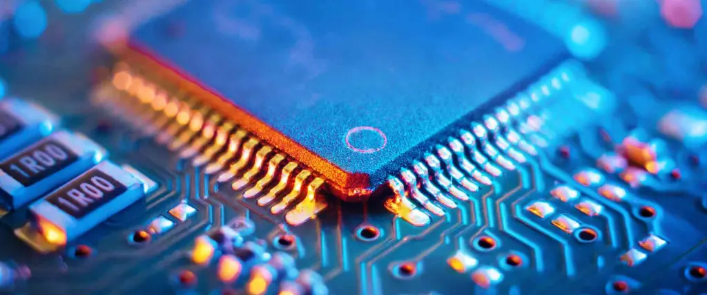
Semiconductor manufacturing is the complex process of fabricating integrated circuits (ICs) on silicon wafers. It involves hundreds of precision steps to build transistor structures layer by layer to create the complex integrated circuits that power electronic devices.
Overview of semiconductor manufacturing process
The key steps in fabricating a semiconductor chip are:
- Wafer fabrication – Producing raw silicon wafers
- Wafer processing – Building transistors and circuits on wafers
- Oxidation – Growing insulating oxide layer
- Photolithography – Transferring circuit pattern onto wafers
- Etching – Removing selected areas of oxide layer
- Ion implantation – Inserting impurity atoms into silicon
- Deposition – Adding thin film material layers
- Chemical mechanical planarization (CMP) – Smoothening wafer surfaces
- Device assembly – Dicing, packaging and interconnect
- Final testing – Verifying and grading ICs according to performance
Advanced semiconductor fabs utilize robotic automation and strict cleanroom environments for precision manufacturing. Let’s look at the key steps in detail.
Wafer fabrication

High purity semiconductor grade silicon is required as the starting material.
Silicon ingot growth
- Ingots grown using Czochralski or Float zone methods to form large single crystal ingots.
- Diameter up to 300mm. Grown as near-perfect monocrystalline material.
Wafer slicing
- Ingots are sliced into discs of required thickness – around 0.7-1 mm.
- Diamond saws used for slicing to prevent silicon contamination.
- Waters used for washing, cooling and catching debris.
Wafer finishing
- Sliced wafers polished mechanically and chemically to achieve mirror finish.
- Processes wafer edges to prevent chipping.
- Cleaning done to remove contaminants.
Wafer testing
- Tests done for material defects like dislocations, oxygen content.
- Checks wafer thickness uniformity, TTV, reflectivity, resistivity.
- Sorts wafers into grades based on quality.
Wafer processing
The sliced silicon wafers undergo hundreds of fabrication steps to build the ICs on them.
Oxidation
Silicon wafers coated with silicon dioxide to provide electrical isolation.
- Thermal oxidation done by heating wafers to 900-1200°C in oxidizing ambient.
- Process forms high quality SiO2 layer of controlled thickness.
- Acts as diffusion mask, isolates devices, reduces surface defects.
Photolithography
Transfers the integrated circuit layout onto the wafers layer by layer. Critical step with high precision requirements.
Photoresist application
- Light sensitive photoresist liquid applied on wafers by spin coating.
- Forms uniform thickness resist film across wafer surface.
Exposure
- Wafers exposed to high intensity UV light through lithography mask containing IC pattern.
- Light causes chemical changes in exposed photoresist regions.
Development
- Chemical treatment dissolves exposed resist regions, transfers mask pattern onto resist.
- Hardened resist remains in unexposed areas, acting as etch mask.

Advanced lithography uses 193nm wavelength UV, immersion techniques to achieve features below 10nm.
Etching
Selectively removes areas not protected by photoresist to transfer pattern onto wafer surface.
Wet etching
- Wafer immersed in liquid etchant that chemically attacks exposed areas.
- Isotropic etch profiles due to etching in all directions.
Dry etching
-Uses reactive ion gases like CF4 for anistropic vertical etching.
- Achieves high precision with reduced undercut.
Etch selectivity ensures desired film is removed without damaging underlying layers.
Ion implantation
- Introduces dopant impurity atoms like boron, phosphorus into silicon wafer.
- Done after lithography to selectively implant regions not masked.
- Creates n-type and p-type regions required to form devices.
Key parameters
- Dopant ion type
- Implant energy – Controls depth of penetration
- Dose – Number of implanted ions per cm2
Activation annealing done post implantation to incorporate dopants.
Deposition
Adds thin layers of insulating and conductive material on wafers through deposition techniques.
Oxidation – To grow oxide layers
Chemical vapor deposition (CVD)
- Reacts gaseous sources to deposit films like polysilicon, silicon nitride.
- Provides conformal high quality films with controllable thickness.
Physical vapor deposition (PVD)
- Evaporates/sputters target material that condenses on wafers.
- Used to deposit metals for interconnects – aluminum, copper.
Atomic layer deposition (ALD)
- Deposits films one atomic layer at a time through sequential reactions.
- Enables thin, conformal films of materials like high-k dielectrics.
Chemical mechanical planarization (CMP)
Flattens wafer surface throughout processing steps for subsequent lithography.
- Chemical slurry reacts with surface material.
- Mechanical buffing removes reacted material.
- Achieves global planarization across the wafer.
These wafer processing steps repeated 20-30 times to build the IC layer by layer.
Device assembly
Completed wafers are diced into individual chips and assembled into packages.
Wafer dicing
- Diamond saws cut along scribe lines to separate individual die.
- Protection films prevent surface damage during dicing process.
Die inspection
- Individual dies tested electrically for defects using test probes.
- Defect mapping done to log exact failure locations.
Die attach
- Functional dies bonded onto lead frames or package substrates using epoxy adhesives.
Wire bonding
- Microscopically thin gold/aluminum wires connected between die bonding pads and package pins.
- Provides electrical connectivity.
- Protective plastic molded over package.
- Only interconnect leads left exposed.
Marking
- Inked dots or text printed on package to identify company, device type, batch number.
Lead finish
- Lead frames plated with solder for SMT assembly, tin for soldering.
Final testing
Before shipping to customers, ICs undergo final tests.
Wafer probing
- Wafers probed before dicing to identify defective die.
- Minimizes packaging known bad parts.
Inline tests
- Automatic testers verify devices at each assembly step – wafer sort, pre-capsulation, final test.
Burn-in
- Devices stressed at high temperature over time to identify early life failures.
Functional testing
- Detailed parametric and functional tests done on automatic test equipment (ATE).
Packaged devices graded based on performance across parameters like speed, power, leakage. Binned into grades.
Conclusion
In summary, semiconductor manufacturing utilizes sophisticated processes like photolithography, etching, doping, deposition to mass produce integrated circuits with transistors below 10 nanometers on 300mm silicon wafers. The complexity of the manufacturing process results in low yield and high fabrication costs. But it enables the exponential advancement of computing power over the decades based on Moore’s Law.
Frequently Asked Questions
Q1. What are the different types of semiconductor device packages?
Some common semiconductor packages are:
- Plastic dual in-line package (PDIP)
- Quad flat pack (QFP)
- Pin grid array (PGA)
- Ball grid array (BGA)
- Ceramic chip carrier
- Chip-scale package (CSP)
- Multi-chip modules (MCM)
Packages connect the silicon die to the printed circuit board.
Q2. What are the key materials used in semiconductor fabrication?
Some key materials used are:
- Silicon – For substrates and growth of oxide
- Photoresists – Light sensitive polymers for lithography
- Dopants – Boron, phosphorus, arsenic for implantation
- Etchants – Acids, plasmas for etching films
- Dielectrics – Silicon dioxide, silicon nitride films
- Metals – Aluminum, copper for interconnects
High purity materials critical for defect reduction.
Q3. What are the main differences between nMOS and CMOS processes?
- nMOS uses only n-channel devices while CMOS uses both nMOS and pMOS devices.
- CMOS utilizes complementary design for logic gates.
- CMOS has much lower static power dissipation than nMOS logic.
- Additional photolithography steps required for pMOS wells in CMOS.
- nMOS simpler process with higher performance but higher power.
Q4. What are some advanced lithography techniques for IC fabrication?
Some advanced techniques used are:
- Immersion lithography – Water fills gap between lens & wafer
- Double patterning – Divides dense patterns into multiple exposures
- Extreme UV lithography – 13.5nm wavelength light source
- Electron beam lithography – Direct electron beam exposure
- Nanoimprint lithography – Physical deformation of resist
Q5. How is mask data prepared for photolithography?
The mask data preparation steps are:
- Circuit layout designed using CAD tools.
- Layout fracturing splits data into mask patterns.
- OPC (optical proximity correction) compensates for optical distortions.
- Mask pattern data exported to fabrication tools.
- Masks fabricated with high accuracy for lithography.
Precision masks are critical to print nanoscale node geometries.