In the realm of Printed Circuit Board (PCB) manufacturing, the uniformity of soldermask thickness plays a crucial role in ensuring the quality, reliability, and performance of electronic devices. One of the key factors influencing this uniformity is the design of the silkscreen printing nail-bed. This article delves into the intricate relationship between nail-bed design and soldermask thickness uniformity, exploring various aspects of this critical manufacturing process.
Understanding Soldermask and Its Importance
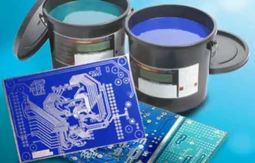
What is Soldermask?
Soldermask, also known as solder resist, is a thin layer of polymer applied to the copper traces of a PCB. Its primary functions include:
- Protecting the copper traces from oxidation
- Preventing solder bridges during the assembly process
- Providing electrical insulation between conductors
- Enhancing the PCB’s aesthetic appearance
Importance of Soldermask Thickness Uniformity
The uniformity of soldermask thickness is critical for several reasons:
| Aspect | Importance | Potential Issues with Non-Uniformity |
| Electrical Performance | Consistent insulation properties | Variations in impedance, signal integrity problems |
| Solder Mask Dam Integrity | Prevents solder bridging | Solder bridges, short circuits |
| Component Placement | Consistent surface for component mounting | Misalignment, poor solder joints |
| Visual Appearance | Professional, high-quality look | Uneven coloration, visible thickness variations |
| Thermal Management | Uniform heat distribution | Hotspots, thermal str |
Silkscreen Printing Process for Soldermask Application
Overview of Silkscreen Printing
Silkscreen printing, also known as screen printing or serigraphy, is a widely used method for applying soldermask to PCBs. The process involves:
- Preparing a screen mesh with the desired pattern
- Applying soldermask ink to the screen
- Using a squeegee to force the ink through the screen onto the PCB
- Curing the applied soldermask
Key Components of Silkscreen Printing
Screen Mesh
The screen mesh is a finely woven fabric (typically made of polyester or stainless steel) stretched over a frame. Its characteristics include:
| Characteristic | Description | Impact on Printing |
| Mesh Count | Number of threads per inch | Affects ink deposit thickness and resolution |
| Thread Diameter | Thickness of individual threads | Influences ink flow and print quality |
| Mesh Tension | Tightness of the mesh on the frame | Affects print accuracy and consisten |
Squeegee
The squeegee is a blade that moves across the screen, forcing ink through the mesh onto the PCB. Important factors include:
- Material (typically polyurethane or rubber)
- Hardness (measured in durometer)
- Profile (straight, beveled, or rounded edge)
- Pressure applied during printing
Soldermask Ink
The soldermask ink is a specially formulated polymer designed for PCB application. Key properties include:
- Viscosity
- Solid content
- Curing method (UV, thermal, or combination)
- Color and opacity
Nail-Bed Design in Silkscreen Printing

What is a Nail-Bed Design?
The nail-bed design refers to the pattern of small, raised points or “nails” on the surface that supports the PCB during the silkscreen printing process. This design is crucial for:
- Minimizing contact area between the support surface and the PCB
- Allowing excess ink to flow away from the print area
- Ensuring uniform pressure distribution during printing
Key Parameters of Nail-Bed Design
| Parameter | Description | Impact on Soldermask Uniformity |
| Nail Density | Number of nails per unit area | Affects support and ink flow |
| Nail Height | Height of individual nails | Influences PCB flatness during printing |
| Nail Shape | Geometry of nail tips (round, flat, conical) | Affects contact area and pressure distribution |
| Nail Pattern | Arrangement of nails (grid, offset, random) | Impacts overall support and uniformit |
Influence of Nail-Bed Design on Soldermask Thickness Uniformity
Pressure Distribution
The nail-bed design significantly affects the distribution of pressure during the printing process:
- Uniform Pressure: A well-designed nail-bed ensures even pressure across the PCB surface, promoting consistent ink deposition.
- Localized Pressure Points: Poorly designed nail-beds can create areas of high pressure, leading to uneven soldermask thickness.
- Edge Effects: The nail pattern near PCB edges can influence soldermask uniformity in these critical areas.
Ink Flow and Evacuation
The nail-bed design also impacts how excess ink flows during and after printing:
- Ink Channeling: Proper nail spacing allows for efficient evacuation of excess ink.
- Ink Pooling: Inadequate spacing can lead to ink pooling, causing thickness variations.
- Edge Accumulation: The nail pattern can influence ink accumulation near PCB edges.
PCB Support and Flatness
Maintaining PCB flatness during printing is crucial for uniform soldermask application:
- Warpage Prevention: An optimal nail-bed design helps prevent PCB warpage during printing.
- Consistent Gap: Proper support ensures a consistent gap between the screen and PCB surface.
- Thin PCB Support: The design must adequately support thin or flexible PCBs without causing deformation.
Optimizing Nail-Bed Design for Soldermask Thickness Uniformity
Nail Density Optimization
Finding the optimal nail density is crucial for balancing support and ink flow:
| Nail Density | Advantages | Disadvantages |
| High Density | Better PCB support, reduced warpage | Limited ink evacuation, potential for pressure points |
| Low Density | Improved ink flow and evacuation | Reduced support, potential for PCB deformation |
| Optimal Density | Balanced support and ink flow | Requires careful design and testing |
Recommendations for nail density optimization:
- Consider PCB thickness and flexibility
- Analyze PCB layout and component density
- Conduct print tests with varying nail densities
- Use computational fluid dynamics (CFD) simulations to predict ink flow
Nail Height and Shape Considerations
The height and shape of individual nails play a significant role in soldermask uniformity:
| Aspect | Considerations | Impact on Uniformity |
| Nail Height | Must accommodate PCB thickness variations | Ensures consistent screen-to-PCB distance |
| Nail Tip Shape | Affects contact area and pressure distribution | Influences local soldermask thickness |
| Nail Profile | Can impact ink flow around nail base | Affects evacuation of excess ink |
Optimization strategies:
- Use adjustable-height nail-beds for different PCB thicknesses
- Experiment with various nail tip shapes (flat, rounded, conical)
- Consider tapered nail profiles to improve ink flow
Nail Pattern Design
The arrangement of nails can significantly influence soldermask uniformity:
| Pattern | Description | Benefits | Challenges |
| Grid | Regular, aligned rows and columns | Predictable support, easy manufacturing | Potential for regular pattern artifacts |
| Offset | Staggered arrangement | Improved ink flow, reduced pattern effects | More complex design and manufacturing |
| Variable Density | Changing density across the bed | Optimized for specific PCB layouts |
Optimization approaches:
- Analyze PCB layout to identify critical areas requiring support
- Use computer-aided design (CAD) tools to optimize nail patterns
- Consider hybrid patterns combining different arrangements
Edge Support Considerations
The nail-bed design near PCB edges requires special attention:
- Enhanced Edge Support: Increase nail density near edges to prevent warpage
- Ink Flow Management: Design channels for ink evacuation along edges
- Adjustable Edge Nails: Implement independently adjustable edge supports
Advanced Techniques for Nail-Bed Design Optimization
Computational Modeling and Simulation
Leveraging computational tools can significantly enhance nail-bed design:
- Finite Element Analysis (FEA):
- Simulate PCB deformation under printing pressure
- Optimize nail placement for minimal warpage
- Computational Fluid Dynamics (CFD):
- Model ink flow through the nail-bed
- Identify areas of potential ink accumulation or insufficient flow
- Multi-physics Simulations:
- Combine mechanical and fluid simulations
- Predict overall impact on soldermask thickness uniformity
Adaptive Nail-Bed Systems
Implementing adaptive systems can accommodate various PCB designs:
- Programmable Nail Heights:
- Adjust individual nail heights based on PCB layout
- Compensate for PCB thickness variations
- Dynamic Pressure Control:
- Implement real-time pressure sensing and adjustment
- Ensure uniform pressure distribution during printing
- Modular Nail-Bed Design:
- Create interchangeable nail-bed sections
- Customize support for different PCB sizes and layouts
Integration with PCB Design Process
Incorporating nail-bed considerations into the PCB design phase:
- Design for Manufacturability (DFM) Guidelines:
- Develop PCB design rules that consider nail-bed support
- Optimize component placement and copper distribution
- Nail-Bed Simulation in PCB Design Software:
- Integrate nail-bed simulation tools with PCB design software
- Predict soldermask uniformity issues during the design phase
- Collaborative Design Approach:
- Foster communication between PCB designers and manufacturing engineers
- Iteratively optimize both PCB and nail-bed designs
Measuring and Monitoring Soldermask Thickness Uniformity

Measurement Techniques
Various methods can be employed to measure soldermask thickness uniformity:
| Technique | Description | Advantages | Limitations |
| Optical Microscopy | Visual inspection of cross-sections | Simple, widely available | Destructive, limited sampling |
| X-ray Fluorescence (XRF) | Non-contact measurement of thickness | Non-destructive, quick | Affected by underlying materials |
| Eddy Current Testing | Measures thickness based on conductivity | Non-destructive, fast | Requires conductive substrate |
| 3D Profilometry | Creates 3D surface map | High resolution, non-contact | Time-consuming for large areas |
Statistical Process Control (SPC)
Implementing SPC for soldermask thickness uniformity:
- Sampling Plans:
- Develop appropriate sampling strategies
- Balance between inspection thoroughness and production efficiency
- Control Charts:
- Monitor thickness measurements over time
- Identify trends and out-of-control situations
- Capability Analysis:
- Calculate process capability indices (Cp, Cpk)
- Ensure process meets specification requirements
Continuous Improvement Strategies
Leveraging measurement data for ongoing optimization:
- Root Cause Analysis:
- Investigate sources of non-uniformity
- Correlate issues with specific nail-bed design parameters
- Design of Experiments (DOE):
- Systematically vary nail-bed design factors
- Identify optimal settings for uniformity
- Machine Learning Approaches:
- Develop predictive models for soldermask uniformity
- Optimize nail-bed designs based on historical data and outcomes
Future Trends and Innovations
Advanced Materials and Processes
Emerging technologies that may impact nail-bed design and soldermask uniformity:
- Novel Soldermask Materials:
- Self-leveling formulations
- Nanotechnology-enhanced polymers
- Alternative Application Methods:
- Inkjet printing of soldermask
- Electrophoretic deposition techniques
- Smart Materials for Nail-Beds:
- Shape-memory alloys for adaptive support
- Self-cleaning surfaces to prevent ink buildup
Industry 4.0 Integration
Incorporating nail-bed optimization into the smart factory concept:
- Real-time Process Monitoring:
- In-line thickness measurements
- Adaptive control of printing parameters
- Digital Twin Technology:
- Virtual modeling of the entire printing process
- Predictive maintenance of nail-beds and printing equipment
- AI-Driven Optimization:
- Machine learning algorithms for continuous process improvement
- Automated design of optimal nail-bed configurations
Conclusion
The design of silkscreen printing nail-beds plays a crucial role in achieving uniform soldermask thickness on PCBs. By carefully considering factors such as nail density, height, shape, and pattern, manufacturers can significantly improve the quality and reliability of their products. As the electronics industry continues to demand higher performance and miniaturization, the importance of optimizing these seemingly small details becomes ever more critical.
The future of nail-bed design lies in the integration of advanced computational tools, adaptive systems, and smart manufacturing concepts. By embracing these technologies and continuously refining their processes, PCB manufacturers can ensure they meet the evolving demands of the electronics industry while maintaining the highest standards of quality and reliability.
Frequently Asked Questions (FAQ)
- Q: How does nail-bed design affect the overall PCB manufacturing process? A: Nail-bed design significantly impacts the silkscreen printing process, which in turn affects soldermask thickness uniformity. This uniformity is crucial for the PCB’s electrical performance, solder mask dam integrity, component placement accuracy, and overall quality. A well-designed nail-bed ensures consistent pressure distribution and proper ink flow, leading to improved manufacturing yield and product reliability.
- Q: What are the most critical parameters to consider when designing a nail-bed for silkscreen printing? A: The most critical parameters include:
- Nail density: Affects support and ink flow
- Nail height: Influences PCB flatness during printing
- Nail shape: Impacts contact area and pressure distribution
- Nail pattern: Affects overall support and uniformity Each of these parameters must be optimized based on the specific PCB design and manufacturing requirements.
- Q: How can manufacturers measure and monitor soldermask thickness uniformity effectively? A: Manufacturers can use various techniques to measure soldermask thickness uniformity:
- Optical microscopy for visual inspection of cross-sections
- X-ray fluorescence (XRF) for non-destructive measurements
- Eddy current testing for quick, non-destructive assessments
- 3D profilometry for high-resolution surface mapping Implementing statistical process control (SPC) with appropriate sampling plans and control charts is crucial for effective monitoring and continuous improvement.
- Q: What role does computational modeling play in nail-bed design optimization? A: Computational modeling plays a significant role in optimizing nail-bed design:
- Finite Element Analysis (FEA) helps simulate PCB deformation under printing pressure
- Computational Fluid Dynamics (CFD) models ink flow through the nail-bed
- Multi-physics simulations combine mechanical and fluid simulations to predict overall impact on soldermask uniformity These tools allow designers to optimize nail-bed configurations virtually, reducing the need for extensive physical prototyping and testing.
- Q: How are emerging technologies and Industry 4.0 concepts influencing nail-bed design and soldermask application? A: Emerging technologies and Industry 4.0 concepts are revolutionizing nail-bed design and soldermask application:
- Advanced materials, such as self-leveling soldermasks and smart nail-bed materials, are being developed
- Real-time process monitoring and adaptive control systems are enabling more precise and consistent printing
- Digital twin technology allows for virtual modeling and optimization of the entire printing process
- AI-driven optimization techniques are being employed for continuous process improvement and automated nail-bed design These advancements are leading to more efficient, flexible, and high-quality PCB manufacturing processes.