In the world of electronics manufacturing, the transition to lead-free soldering has brought about numerous challenges and considerations. One of the most critical aspects of this shift is the impact of higher soldering temperatures on printed circuit boards (PCBs) and their components. As lead-free solders typically require higher melting points compared to traditional lead-based solders, the question of how often a PCB can be exposed to these elevated temperatures has become increasingly important.
This comprehensive article will explore the factors influencing the thermal resilience of PCBs, the effects of repeated exposure to lead-free soldering temperatures, and best practices for managing thermal stress in PCB assembly and rework processes. By understanding these aspects, manufacturers can optimize their processes to ensure the reliability and longevity of their electronic products.
Understanding Lead-free Soldering Temperatures
The Shift to Lead-free Soldering
The global electronics industry has been moving away from lead-based solders due to environmental and health concerns. This transition has necessitated the use of alternative solder alloys, most of which require higher processing temperatures.
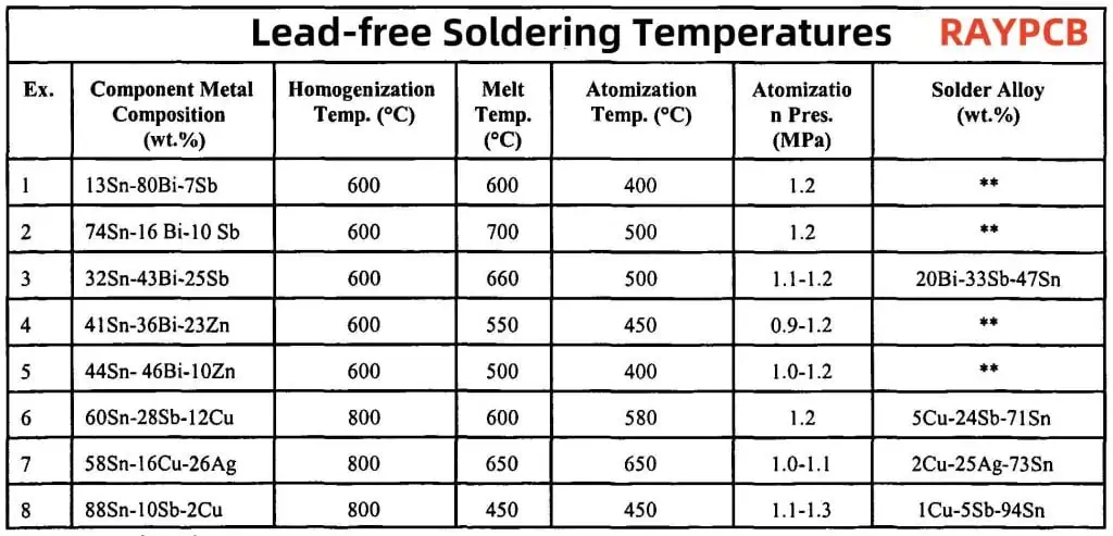
Typical Lead-free Soldering Temperatures
Lead-free solders generally have higher melting points compared to traditional tin-lead solders. Here’s a comparison of common solder alloys and their melting points:
| Solder Type | Composition | Melting Point (°C) |
| Tin-Lead (SnPb) | 63% Sn, 37% Pb | 183 |
| SAC305 (Lead-free) | 96.5% Sn, 3% Ag, 0.5% Cu | 217-220 |
| SAC405 (Lead-free) | 95.5% Sn, 4% Ag, 0.5% Cu | 217-220 |
| SN100C (Lead-free) | 99.3% Sn, 0.7% Cu, Ni, Ge | 227 |
As evident from the table, lead-free solders typically require temperatures 30-40°C higher than traditional lead-based solders during the reflow process.
Factors Affecting PCB Thermal Resilience
Several factors influence how well a PCB can withstand repeated exposure to lead-free soldering temperatures:
1. PCB Material Properties
Glass Transition Temperature (Tg)
The glass transition temperature (Tg) is a critical property of PCB materials. It represents the temperature at which the material begins to soften and transition from a rigid to a more pliable state.
| PCB Material | Typical Tg Range (°C) |
| FR-4 (Standard) | 130-140 |
| High-Tg FR-4 | 170-180 |
| Polyimide | >250 |
PCBs with higher Tg values generally exhibit better resistance to thermal stress and can withstand more reflow cycles.
Coefficient of Thermal Expansion (CTE)
The CTE describes how much a material expands or contracts with temperature changes. Mismatches in CTE between different PCB materials and components can lead to stress and potential failure during thermal cycling.
2. PCB Design and Construction
Layer Count and Thickness
Thicker, multi-layer PCBs generally have better thermal distribution and can withstand more reflow cycles compared to thinner, single-layer boards.
Copper Distribution
Even distribution of copper across the PCB layers helps in uniform heat distribution, reducing the risk of localized thermal stress.
Via Design
Proper via design, including the use of thermal relief vias, can help manage heat dissipation during the soldering process.
3. Component Properties
Component Thermal Sensitivity
Different components have varying levels of thermal sensitivity. For example, electrolytic capacitors are generally more sensitive to high temperatures compared to ceramic capacitors.
Package Type
The type of component package (e.g., BGA, QFP, SMD) can affect its ability to withstand repeated thermal cycles.
4. Soldering Process Parameters
Peak Temperature
The maximum temperature reached during the reflow process significantly impacts the thermal stress on the PCB and components.
Time Above Liquidus (TAL)
The duration for which the PCB is exposed to temperatures above the solder’s melting point affects the cumulative thermal stress.
Heating and Cooling Rates
Rapid temperature changes can induce thermal shock, potentially leading to PCB or component damage.
Effects of Repeated Exposure to Lead-free Soldering Temperatures
Subjecting a PCB to multiple lead-free soldering cycles can have various effects on its integrity and reliability:
1. PCB Delamination
Repeated thermal stress can cause separation between the layers of a multi-layer PCB, leading to delamination.
2. Pad Cratering
High temperatures and thermal cycling can cause microcracks in the resin between copper pads and the PCB substrate.
3. Component Damage
Sensitive components may suffer internal damage or degradation due to repeated exposure to high temperatures.
4. Solder Joint Reliability
Multiple reflow cycles can affect the reliability of solder joints, potentially leading to weak or brittle connections.
5. Warpage
PCB warpage can occur due to CTE mismatches and cumulative thermal stress, affecting component placement and overall board functionality.
Guidelines for Multiple Reflow Cycles
While the exact number of times a PCB can be safely exposed to lead-free soldering temperatures varies depending on the factors mentioned earlier, here are some general guidelines:
Standard FR-4 PCBs
For typical FR-4 PCBs, it’s generally recommended to limit the number of reflow cycles to 3-5 times.
High-Tg FR-4 PCBs
High-Tg FR-4 boards may withstand 5-7 reflow cycles, depending on the specific material properties and design.
Polyimide PCBs
Polyimide PCBs, due to their higher temperature resistance, can potentially undergo 7-10 reflow cycles.
It’s important to note that these are general guidelines, and actual limits should be determined through testing and validation for specific PCB designs and applications.
Best Practices for Managing Thermal Stress

To maximize the number of times a PCB can be safely exposed to lead-free soldering temperatures, consider the following best practices:
1. Material Selection
Choose PCB materials with appropriate Tg values and thermal properties for your application.
2. Thermal Profiling
Develop and optimize reflow profiles to minimize thermal stress while ensuring proper solder joint formation.
3. Component Placement
Consider the thermal sensitivity of components when designing the PCB layout.
4. Use of Thermal Relief Pads
Implement thermal relief pads to manage heat distribution and reduce thermal stress on sensitive components.
5. Preheating and Controlled Cooling
Incorporate gradual preheating and controlled cooling stages in the reflow profile to minimize thermal shock.
6. Nitrogen Atmosphere
Consider using a nitrogen atmosphere during reflow, which can allow for lower peak temperatures and shorter TAL.
7. Rework Strategies
Develop strategies to minimize the number of rework cycles required, such as using selective soldering techniques for repairs.
8. Thermal Simulation
Utilize thermal simulation tools to predict and optimize heat distribution across the PCB during the reflow process.
Monitoring and Testing
To ensure PCB reliability after multiple lead-free soldering cycles, implement the following monitoring and testing procedures:
1. X-ray Inspection
Use X-ray inspection to detect internal defects such as voids or cracks that may develop after multiple reflow cycles.
2. Thermal Cycling Tests
Conduct thermal cycling tests to evaluate the long-term reliability of PCBs and components after repeated exposure to high temperatures.
3. Cross-sectioning Analysis
Perform cross-sectioning analysis to examine the internal structure of PCBs and solder joints for signs of degradation.
4. Electrical Testing
Implement comprehensive electrical testing to ensure functionality and performance after each reflow cycle.
5. Warpage Measurement
Use warpage measurement techniques to assess the cumulative effects of thermal stress on PCB flatness.
Conclusion
The question of how often a PCB can be raised to lead-free soldering temperatures does not have a one-size-fits-all answer. It depends on a complex interplay of factors including PCB material properties, design considerations, component characteristics, and process parameters. While general guidelines suggest limiting reflow cycles to 3-10 times depending on the PCB material, the actual limit for a specific design should be determined through careful testing and validation.
By understanding the factors affecting PCB thermal resilience, implementing best practices for managing thermal stress, and utilizing appropriate monitoring and testing procedures, manufacturers can optimize their processes to maximize PCB reliability while meeting the challenges of lead-free soldering. As the electronics industry continues to evolve, ongoing research and development in PCB materials and manufacturing techniques will likely lead to further improvements in thermal resilience and reliability.
Frequently Asked Questions (FAQ)
1. Can I use the same reflow profile for all lead-free PCB assemblies?
While a general lead-free reflow profile can serve as a starting point, it’s not recommended to use the exact same profile for all PCB assemblies. Each PCB design may require a tailored reflow profile due to variations in:
- Board thickness and layer count
- Component mix and thermal mass
- Solder paste composition
- PCB material properties
It’s best practice to develop and optimize a specific reflow profile for each PCB design, considering factors such as:
- Ramp rates (heating and cooling)
- Soak times and temperatures
- Peak temperature and time above liquidus
- Overall thermal budget
Using thermal profiling equipment and software can help in developing and fine-tuning reflow profiles for specific PCB assemblies, ensuring optimal solder joint formation while minimizing thermal stress on the board and components.
2. How does the use of mixed technology (through-hole and SMT components) affect the number of allowable reflow cycles?
The use of mixed technology on a PCB can complicate the reflow process and potentially limit the number of allowable reflow cycles. This is due to several factors:
- Thermal mass differences: Through-hole components typically have higher thermal mass than SMT components, leading to uneven heating and cooling across the board.
- Heat exposure for through-hole components: When SMT components are reflowed, through-hole components are also exposed to high temperatures, potentially exceeding their rated limits.
- Stress on plated through-holes: Repeated thermal cycling can cause stress on plated through-holes, potentially leading to barrel cracks or pad lifting.
- Flux residues: Multiple reflow cycles can lead to accumulation of flux residues, particularly in through-hole areas, affecting cleanliness and potentially long-term reliability.
To manage these challenges:
- Consider using a selective soldering process for through-hole components after SMT reflow.
- Optimize component placement to balance thermal distribution.
- Use thermally robust PCB materials and design techniques.
- Implement strict process controls and thermal profiling.
Generally, mixed technology boards may require more conservative limits on the number of reflow cycles compared to pure SMT assemblies. Thorough testing and validation are crucial to determine safe limits for specific designs.
3. What are the signs that a PCB has been exposed to too many reflow cycles?
Several indicators can suggest that a PCB has been subjected to excessive thermal stress from multiple reflow cycles:
- Visual indicators:
- Discoloration or browning of the PCB substrate
- Measurable warpage or twisting of the board
- Lifted or separated pads
- Cracks in the solder mask
- Structural issues:
- Delamination between PCB layers (detectable via microsection analysis or ultrasonic inspection)
- Barrel cracks in plated through-holes
- Pad cratering (separation of pads from the laminate)
- Solder joint problems:
- Excessive intermetallic compound (IMC) growth
- Brittle or cracked solder joints
- Voiding in solder joints
- Component issues:
- Package deformation or cracking
- Internal damage to sensitive components (e.g., delamination in MLCCs)
- Electrical problems:
- Intermittent connections
- Changes in impedance characteristics
- Increased leakage currents
- Performance degradation:
- Shifts in electrical parameters
- Reduced reliability or lifespan of the assembly
Regular inspection, both visual and using advanced techniques like X-ray and thermal imaging, can help detect these issues early. If any of these signs are observed, it may indicate that the PCB has reached or exceeded its safe limit for reflow cycles.
4. How does the transition to lead-free soldering affect the rework process for PCBs?
The transition to lead-free soldering has significantly impacted the rework process for PCBs in several ways:
- Higher temperatures:
- Lead-free solders require higher rework temperatures, increasing the risk of thermal damage to PCBs and components.
- More precise temperature control is necessary during rework.
- Narrower process window:
- The temperature range between solder melting and component damage is smaller, requiring more precise heating methods.
- Different solder behavior:
- Lead-free solders often have poorer wetting characteristics, making rework more challenging.
- The higher surface tension of lead-free solders can make it harder to remove components.
- Component considerations:
- Some components may not be rated for multiple exposures to lead-free reflow temperatures, limiting rework options.
- Equipment and tooling:
- Rework stations may need upgrading to handle higher temperatures and provide more precise control.
- Specialized nozzles and tooling may be required for effective lead-free rework.
- Increased risk of PCB damage:
- Higher temperatures increase the risk of pad lifting, delamination, and other thermal damage during rework.
- Flux considerations:
- Different flux formulations may be necessary to work effectively with lead-free solders at higher temperatures.
- Inspection and quality control:
- More rigorous inspection may be required after rework due to the increased risks associated with higher temperatures.
To address these challenges:
- Develop specific rework profiles for lead-free assemblies.
- Invest in advanced rework equipment with precise temperature control.
- Train technicians on lead-free rework techniques.
- Consider using localized heating methods to minimize overall thermal exposure.
- Implement strict thermal profiling and monitoring during rework processes.
By adapting rework processes and equipment to the requirements of lead-free soldering, manufacturers can maintain high-quality standards while managing the increased thermal risks associated with lead-free rework.
5. Are there any emerging technologies or materials that can increase a PCB’s tolerance to multiple reflow cycles?
Yes, several emerging technologies and materials are being developed to enhance PCB tolerance to multiple reflow cycles:
- Advanced PCB Materials:
- Ultra-high Tg laminates (>200°C) for improved thermal stability.
- Low-loss materials with better thermal conductivity.
- Ceramic-filled composites for enhanced thermal management.
- Thermal Management Technologies:
- Embedded heat-spreading layers (e.g., copper coins, thermal vias).
- Phase-change materials for temperature regulation during reflow.
- Component Packaging:
- Advanced thermal interface materials for better heat dissipation.
- Hermetically sealed packages for sensitive components.
- Solder Alloy Developments:
- New lead-free alloys with lower melting points and improved reliability.
- Nano-reinforced solders for enhanced mechanical properties.
- Process Innovations:
- Selective laser soldering for localized heating.
- Vapor phase soldering for more uniform heat distribution.
- Design for Thermal Management:
- AI-driven PCB layout optimization for better thermal distribution.
- Integrated thermal simulation in PCB design software.
- Coating Technologies:
- Advanced conformal coatings that provide thermal protection.
- Nano-coatings for improved heat dissipation.
- Flexible and Stretchable Electronics:
- Materials that can better withstand thermal cycling due to their inherent flexibility.
- Additive Manufacturing:
- 3D-printed PCB structures with integrated thermal management features.
- Self-healing Materials:
- Polymers with self-healing properties to mitigate micro-cracks caused by thermal stress.
While many of these technologies are still in development or early adoption stages, they show promise in increasing PCB resilience to multiple reflow cycles. As these innovations mature and become more widely adopted, they have the potential to significantly improve PCB reliability in lead-free soldering processes.
It’s important to note that the effectiveness and applicability of these technologies can vary depending on specific PCB designs and manufacturing requirements. Thorough testing and validation are necessary before implementing any new materials or processes in production environments.