Flexible Printed Circuit Boards (Flex PCBs) have revolutionized electronic design, offering lightweight, space-saving solutions for various applications. Understanding the intricacies of Flex PCB stackup design is crucial for engineers and designers aiming to optimize their products. This article delves into the world of Flex PCB stackups, exploring configurations from 1 to 8 layers.

1. What is a Flex PCB Stackup?
Definition and Basics
A flex PCB stackup refers to the arrangement of conductive and insulating layers that make up a flexible printed circuit board. This layered structure is what allows the circuit to bend and flex while maintaining electrical integrity. The stackup design is crucial as it directly impacts the circuit’s mechanical properties, electrical performance, and overall reliability.
Differences Between Rigid, Flex, and Rigid-Flex PCB Stackups
While rigid PCBs are composed of stiff materials like FR-4, flex PCBs use flexible substrates that allow for bending and folding. The key differences are:
- Rigid PCBs: Typically use FR-4 or similar materials, with copper layers sandwiched between insulating layers. They’re inflexible and designed for static applications.
- Flex PCBs: Utilize flexible materials like polyimide for the base substrate, allowing the circuit to bend. They can have single or multiple layers.
- Rigid-Flex PCBs: Combine areas of rigid and flexible PCB technology on a single board, offering the best of both worlds for complex applications.
Key Materials Used in Flex PCB Stackups
The primary materials used in flex PCB stackups include:
- Polyimide: The most common base substrate for flex circuits, known for its excellent flexibility, heat resistance, and dimensional stability.
- Adhesive: Used to bond conductive layers to the substrate. Some advanced designs use adhesiveless constructions for improved flexibility and thermal performance.
- Coverlay: A protective layer applied over the outer copper layers, similar to solder mask on rigid PCBs but more flexible.
- Copper: The conductive material used for circuit traces, available in various weights to balance flexibility and current-carrying capacity.
Understanding these materials and their properties is essential for creating an optimal flex PCB stackup design.
2. Importance of Proper Flex PCB Layer Stackup
Balancing Mechanical Flexibility and Electrical Performance
One of the primary challenges in flex PCB stackup design is striking the right balance between mechanical flexibility and electrical performance. A well-designed stackup must:
- Allow for the required degree of flexing without damaging the circuit.
- Maintain signal integrity across bending regions.
- Provide adequate shielding and impedance control for high-speed signals.
Achieving this balance often involves careful material selection, layer ordering, and thickness considerations.
Impact on Bend Radius, Durability, and Signal Integrity
The stackup design directly affects the circuit’s minimum bend radius – the smallest curve the PCB can conform to without damage. A properly designed stackup can:
- Minimize stress on copper traces during flexing.
- Reduce the risk of delamination or cracking in dynamic applications.
- Maintain consistent electrical characteristics even when bent.
For instance, placing signal layers closer to the neutral axis (the center of the stackup) can reduce strain during bending, improving durability.
How Flex Circuit Stackup Affects Product Lifespan
The longevity of a flexible circuit is intrinsically tied to its stackup design. A well-engineered stackup can significantly extend a product’s lifespan by:
- Reducing mechanical stress on components and solder joints.
- Minimizing signal degradation over time due to repeated flexing.
- Improving resistance to environmental factors like temperature fluctuations and humidity.
3. Typical Flex PCB Stackup Structures
Flex PCB stackups refer to the arrangement of conductive layers, insulating materials, and other elements that make up a flexible circuit board. The design of these stackups is critical in determining the board’s performance, flexibility, and reliability.
1 Layer Flex PCB Stackup
The simplest form of Flex PCB, a single-layer design consists of:
- Coverlay (optional)
- Single conductive layer (usually copper)
- Flexible base material (e.g., Polyimide)
- Coverlay (optional)

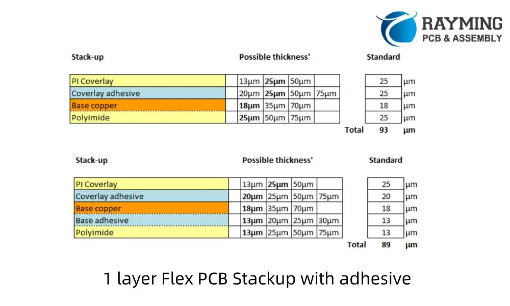
This configuration is ideal for simple circuits with low component density. It offers maximum flexibility and is cost-effective for basic applications.
Read more about:
2 Layer Flex PCB Stackup
A 2-layer Flex PCB stackup typically includes:
- Coverlay
- Conductive layer
- Flexible base material
- Conductive layer
- Coverlay
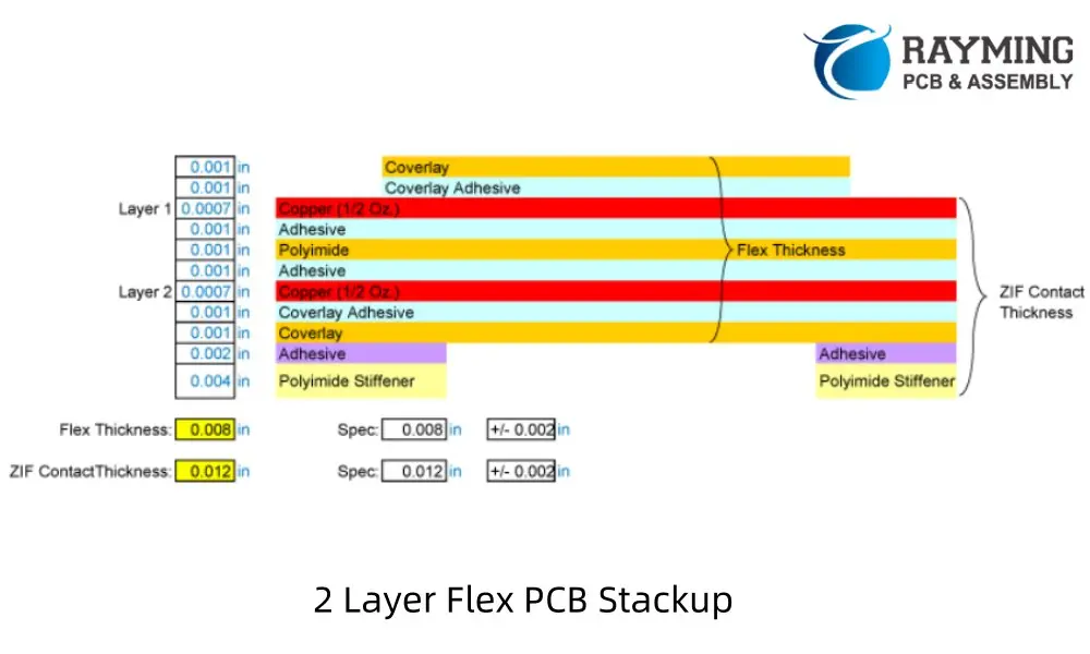
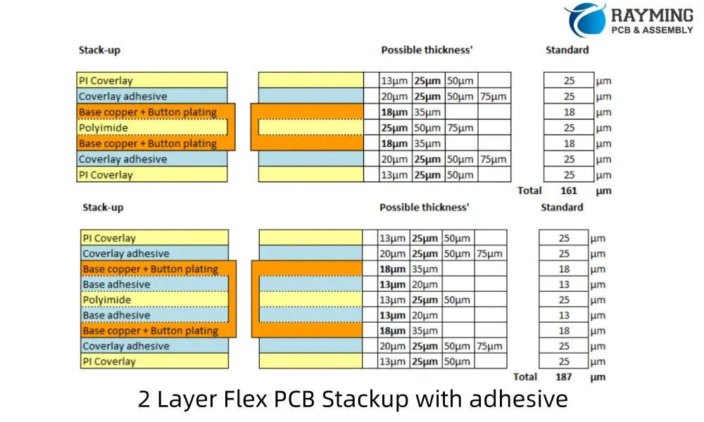
This design allows for more complex circuits while maintaining good flexibility. It’s commonly used in applications requiring ground planes or power distribution.
4 Layer Flex PCB Stackup
A 4-layer Flex PCB stackup usually consists of:
- Coverlay
- Conductive layer
- Flexible base material
- Conductive layer
- Flexible base material
- Conductive layer
- Flexible base material
- Conductive layer
- Coverlay

This configuration offers increased circuit density and improved signal integrity. It’s suitable for applications requiring separation of analog and digital signals or complex routing.
6 Layer Flex PCB Stackup
A typical 6-layer Flex PCB stackup includes:
- Coverlay
- Conductive layer
- Flexible base material
- Conductive layer
- Flexible base material
- Conductive layer
- Flexible base material
- Conductive layer
- Flexible base material
- Conductive layer
- Flexible base material
- Conductive layer
- Coverlay

This design allows for high component density and is ideal for complex circuits requiring multiple ground and power planes. It offers excellent signal integrity but with reduced flexibility compared to lower layer counts.
8 Layer Flex PCB Stackup
An 8-layer Flex PCB stackup typically consists of:
- Coverlay
- Conductive layer
- Flexible base material
- Conductive layer
- Flexible base material
- Conductive layer
- Flexible base material
- Conductive layer
- Flexible base material
- Conductive layer
- Flexible base material
- Conductive layer
- Flexible base material
- Conductive layer
- Flexible base material
- Conductive layer
- Coverlay
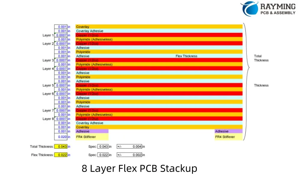
This configuration is used for the most complex flex circuits, offering maximum circuit density and signal integrity. However, it has the least flexibility among the options discussed.
4. 4 Layer Flex PCB Stackup: Advanced Designs
Common Architecture for 4 Layer Flex PCB Stackup
A typical 4 layer flex PCB stackup might be structured as follows:
- Top coverlay
- Signal layer 1
- Ground plane
- Power plane
- Signal layer 2
- Bottom coverlay
This arrangement allows for optimal signal integrity and power distribution while maintaining flexibility.
Importance of Symmetrical Stackup for Dynamic Flexing
Symmetry in the stackup design is crucial for dynamic flexing applications. A symmetrical design:
- Balances stress across the layers during bending
- Reduces the risk of warping or twisting
- Maintains consistent electrical properties in different flex states
To achieve symmetry, designers often mirror the stackup around the central core, using similar materials and thicknesses on both sides.
Via Management and Controlled Impedance Considerations
In 4 layer flex PCB stackups, via management becomes more complex. Some key considerations include:
- Minimizing via use in flex areas to maintain bendability
- Using buried or blind vias to increase routing density without compromising flexibility
- Implementing teardrops at via-to-trace connections to improve reliability
Controlled impedance is often a requirement in high-speed designs. In a 4 layer stackup, designers can:
- Use the inner layers for uninterrupted ground and power planes
- Adjust trace width and spacing on outer layers to achieve desired impedance
- Utilize electromagnetic field simulation tools to fine-tune impedance control
5. Special Considerations for Flex Stackup Design
How to Minimize Stress and Avoid Cracking
To ensure the longevity of flex PCBs, designers must minimize stress on the copper traces and substrate. Key strategies include:
- Using rolled annealed copper instead of electrodeposited copper for better flex endurance
- Implementing teardrop-shaped pads to reduce stress concentration
- Orienting traces perpendicular to the bend axis in flex areas
- Using smaller trace widths in areas of high stress
Coverlay vs. Soldermask Choice in Flex Stackup
While rigid PCBs typically use soldermask, flex PCBs often employ coverlay for outer layer protection. The choice between coverlay and soldermask depends on several factors:
Coverlay Advantages:
- Better flexibility and durability
- Excellent chemical resistance
- Uniform thickness for improved impedance control
Soldermask Advantages:
- Lower cost
- Easier application in small areas
- Better for fine-pitch components
For dynamic flex applications, coverlay is generally preferred due to its superior flexibility and durability.
Adhesiveless Constructions
Adhesiveless flex PCB constructions are gaining popularity due to several advantages:
- Improved flexibility and bend radius capabilities
- Better thermal performance
- Reduced overall thickness
- Enhanced electrical performance due to lower dielectric constant
However, adhesiveless constructions can be more challenging to manufacture and may have higher initial costs. The choice between adhesive-based and adhesiveless constructions should be based on the specific requirements of the application.
6. Tools and Resources for Flex Circuit Stackup Design
How Altium Flex Stackup Tools Assist with Design Simulation
Altium Designer, a popular PCB design software, offers powerful tools for flex PCB stackup design and simulation. Key features include:
- Layer Stack Manager: Allows designers to define and visualize the PCB stackup, including flex layers.
- Flex and Rigid-Flex Support: Enables the definition of flex and rigid regions within the same design.
- 3D PCB Visualization: Helps in understanding how the flex PCB will behave in its bent state.
- Signal Integrity Analysis: Allows for impedance calculations and signal integrity simulations specific to flex designs.
Typical Workflow: Setting Bend Parameters, Defining Flex Regions
A typical workflow for flex PCB design in Altium might include:
- Define the overall stackup using the Layer Stack Manager.
- Specify flex and rigid regions using the Rigid-Flex Editor.
- Set bend lines and bend parameters (e.g., bend radius, bend angle).
- Route traces with consideration for bend regions.
- Perform design rule checks specific to flex PCBs.
- Run signal integrity simulations to ensure performance in both flat and bent states.
- Generate 3D models and documentation for manufacturing.
By leveraging these tools, designers can catch potential issues early in the design process, saving time and reducing the risk of costly revisions.
7. Manufacturer-Specific Stackups: PCBWay Flex PCB Stackup Options
Overview of PCBWay Flex Stackup Capabilities
PCBWay, a leading PCB manufacturer, offers a wide range of flex PCB stackup options to cater to diverse design requirements. Their capabilities include:
- Single-layer to multi-layer flex PCBs (up to 8 layers)
- Various substrate materials, including polyimide and PET
- Different copper weights (0.5oz to 2oz)
- Adhesive-based and adhesiveless constructions
- Coverlay and soldermask options
PCBWay’s advanced manufacturing processes allow for:
- Minimum trace width/spacing down to 3mil/3mil
- Laser-drilled microvias for high-density designs
- Selective stiffener application for hybrid flex-rigid designs
Tips on Communicating with Manufacturers about PCBWay Flex PCB Stackup Requirements
Effective communication with manufacturers like PCBWay is crucial for successful flex PCB production. Here are some tips:
- Provide Detailed Stackup Information:
- Clearly specify layer count, materials, and thicknesses
- Indicate which layers are flexible and which (if any) are rigid
- Define Bend Requirements:
- Specify minimum bend radius
- Indicate whether the flex is for dynamic or static applications
- Clarify Special Requirements:
- Controlled impedance needs
- Any specific material preferences (e.g., adhesiveless construction)
- Supply Detailed Documentation:
- Provide Gerber files, drill files, and fabrication drawings
- Include a readme file with any special instructions or requirements
- Discuss Prototyping Options:
- Consider ordering prototypes before full production
- Discuss any testing or validation requirements
- Leverage Manufacturer Expertise:
- Ask for recommendations on improving manufacturability
- Inquire about alternative materials or processes that might enhance performance or reduce cost
By following these guidelines, you can ensure that your flex PCB design intent is clearly communicated, leading to a smoother manufacturing process and a higher-quality end product.
8. Best Practices for a Reliable Flex PCB Stackup
Layer Symmetry
Maintaining symmetry in the flex PCB stackup is crucial for preventing warpage and ensuring consistent performance. Best practices include:
- Balancing copper weights on both sides of the core
- Mirroring layer structures around the central core
- Using an odd number of layers with a central ground plane for better EMI performance
Proper Material Selection
Choosing the right materials is fundamental to a successful flex PCB design:
- Substrate: Polyimide is the most common choice due to its excellent flexibility and temperature resistance. For less demanding applications, PET might be suitable.
- Copper Foil: Rolled annealed copper offers better flex endurance than electrodeposited copper.
- Adhesives: Choose adhesives that maintain flexibility over the product’s lifetime and temperature range.
- Coverlay: Select a coverlay material that matches the flexibility of your substrate.
Bend Area Design Rules
Optimizing the design for bend areas is critical for long-term reliability:
- Route traces perpendicular to the bend line whenever possible.
- Use smaller trace widths in bend areas to reduce stress.
- Avoid placing vias or components directly in bend zones.
- Implement teardrop-shaped pads to reduce stress concentration.
- Consider using curved traces instead of sharp corners in high-stress areas.
Controlled Impedance for High-Speed Signals
For high-speed applications, maintaining controlled impedance is crucial:
- Use continuous ground planes adjacent to signal layers.
- Carefully calculate and maintain consistent trace width and spacing.
- Consider using impedance-controlled microstrip or stripline configurations.
- Use electromagnetic simulation tools to verify impedance control across bend areas.
By adhering to these best practices, designers can create flex PCB stackups that offer optimal performance, reliability, and manufacturability.
9. Conclusion
The world of flexible electronics continues to expand, pushing the boundaries of what’s possible in product design and functionality. At the heart of this revolution lies the critical importance of a well-designed flex PCB stackup. As we’ve explored throughout this article, the stackup is not merely a technical specification but the foundation upon which reliable, high-performance flexible circuits are built.
From single-layer designs to complex multi-layer architectures, each flex PCB stackup presents unique challenges and opportunities. By understanding the fundamental principles of stackup design – from material selection and layer