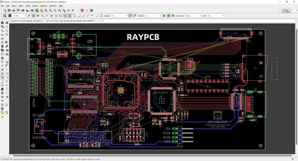
Express PCB and Express SCH represent a powerful combination of circuit design tools that have become popular among electronics engineers, hobbyists, and professional designers. This comprehensive guide explores both software packages, their features, capabilities, and how they work together to streamline the electronic design process.

Express SCH Overview
Core Features and Capabilities
| Feature Category | Description | Benefits |
| Component Library | Over 10,000 built-in components | Quick start for common designs |
| Custom Components | User-defined symbol creation | Flexibility for specialized needs |
| Net Labels | Automated connectivity tracking | Reduces wiring errors |
| Multi-page Support | Up to 100 pages per design | Handles complex projects |
| Export Options | PDF, PNG, BMP formats | Easy documentation |
User Interface Elements
| UI Element | Function | Access Method |
| Component Browser | Browse and select parts | Left sidebar |
| Properties Panel | Edit component parameters | Right-click menu |
| Drawing Tools | Create custom symbols | Top toolbar |
| Sheet Navigator | Switch between pages | Bottom panel |
| Net Manager | View and edit connections | Tools menu |
Express PCB Features

Board Design Capabilities
| Feature | Specification | Limitations |
| Maximum Board Size | 31″ x 31″ | Single-sided view |
| Layer Support | Up to 4 layers | No blind/buried vias |
| Minimum Trace Width | 6 mil | Manufacturing dependent |
| Grid Resolution | 0.001 inch | Fixed metric conversion |
| Component Spacing | 0.025 inch minimum | DRC recommended |
Manufacturing Specifications
| Parameter | Standard Option | Premium Option |
| Copper Weight | 1 oz | 2 oz available |
| Minimum Hole Size | 0.020″ | 0.013″ |
| Silkscreen | Both sides | High resolution |
| Solder Mask | Green standard | Multiple colors |
| Turn-around Time | 3-5 days | 24-hour available |
Integration Between Express SCH and PCB
Data Transfer Workflow
| Step | Process | Verification |
| Schematic Complete | Design verification | DRC check |
| Component Association | Link SCH to PCB footprints | Library check |
| Net List Generation | Automatic creation | Connectivity review |
| PCB Import | Component placement | Layout verification |
| Final Check | Design rule verification | Manufacturing review |
Design Process Best Practices
Project Setup Guidelines
Schematic Design Phase
| Task | Recommendation | Common Pitfalls |
| Page Setup | Start with main sheet | Inconsistent sheet sizes |
| Component Selection | Use standard parts first | Custom part errors |
| Power Distribution | Define early | Ground loop issues |
| Signal Routing | Group similar signals | Noise coupling |
| Documentation | Add notes during design | Missing information |
PCB Layout Phase
| Stage | Focus Areas | Quality Checks |
| Component Placement | Power flow optimization | Thermal considerations |
| Layer Stack | Signal integrity | Impedance control |
| Routing Strategy | Critical paths first | DRC compliance |
| Thermal Management | Heat dissipation | Component spacing |
| Manufacturing Review | DFM guidelines | Cost optimization |
Advanced Features and Techniques
Custom Library Development
| Element Type | Creation Method | Verification Steps |
| Schematic Symbols | Vector drawing tools | Pin mapping check |
| PCB Footprints | Dimension input | Pad spacing review |
| Combined Devices | Library linking | Association test |
| Custom Packages | 3D modeling support | Manufacturing check |
Design Rule Implementation
| Rule Category | Parameters | Verification Method |
| Clearance | Trace-to-trace spacing | DRC check |
| Hole Size | Drill specifications | Manufacturing limits |
| Copper Width | Current capacity | Thermal analysis |
| Layer Rules | Stack-up requirements | Signal integrity |
Performance Optimization

System Requirements
| Component | Minimum | Recommended |
| Processor | 1.5 GHz | 3+ GHz |
| RAM | 4 GB | 8+ GB |
| Storage | 500 MB | 2+ GB |
| Display | 1366×768 | 1920×1080 |
| OS Support | Windows 7 | Windows 10/11 |
Software Performance Tips
| Area | Optimization | Impact |
| File Management | Regular saving | Data protection |
| Memory Usage | Background apps | Speed improvement |
| Graphics | Hardware acceleration | Smooth rendering |
| Backup | Automated backups | Design security |
Cost Considerations
Licensing Options
| License Type | Features | Price Range |
| Basic | Essential tools | Free |
| Standard | Full feature set | $100-200 |
| Professional | Advanced capabilities | $200-500 |
| Enterprise | Multi-user support | Custom |
Manufacturing Cost Factors
| Factor | Impact | Optimization |
| Board Size | Direct cost correlation | Efficient layout |
| Layer Count | Exponential cost increase | Layer optimization |
| Component Density | Assembly complexity | Strategic placement |
| Special Requirements | Additional processing | Design alternatives |
Future Development and Updates
Planned Features
| Feature Category | Expected Implementation | Benefits |
| Cloud Integration | Next major release | Remote collaboration |
| AI Assisted Routing | Development phase | Layout optimization |
| 3D Visualization | Beta testing | Design verification |
| Advanced DRC | Upcoming update | Error reduction |
Frequently Asked Questions (FAQ)
Q1: Can Express PCB and Express SCH files be exported to other CAD software?
A1: Express PCB and Express SCH use proprietary file formats, but they offer limited export capabilities. Schematics can be exported as PDF or image files, while PCB designs can be exported as Gerber files for manufacturing. However, direct conversion to other CAD formats is not supported.
Q2: What are the limitations of the free version compared to the paid versions?
A2: The free version includes basic schematic and PCB design capabilities but has limitations on:
- Board size (maximum 4″ x 4″)
- Layer count (2 layers maximum)
- Export options (limited file formats)
- Advanced features (no auto-routing or DRC) Paid versions remove these restrictions and add professional features.
Q3: How does the auto-routing capability compare to other PCB design software?
A3: Express PCB’s auto-routing functionality is basic compared to professional tools like Altium or KiCad. It works well for simple designs but may struggle with:
- High-density boards
- Complex routing rules
- Mixed-signal designs Manual routing is recommended for critical signals and complex layouts.
Q4: Can I create custom component libraries in Express SCH and PCB?
A4: Yes, both Express SCH and PCB support custom component creation. The process involves:
- Creating the schematic symbol in Express SCH
- Designing the PCB footprint in Express PCB
- Linking the components through the library manager
- Validating the new component in test designs
Q5: How reliable is the integration between Express SCH and PCB?
A5: The integration between Express SCH and PCB is generally reliable for basic to moderate complexity designs. Key considerations include:
- Component associations must be properly defined
- Net names must be consistent
- Manual verification of the transfer is recommended
- Complex designs may require additional checking Regular saving and backup of both files is recommended during the transfer process.
