Electroplated nickel has become an integral part of modern printed circuit board (PCB) manufacturing, offering enhanced durability, conductivity, and corrosion resistance. This comprehensive guide explores the technical aspects, processes, and considerations involved in nickel electroplating for PCBs, providing manufacturers and engineers with essential information for optimal implementation.

Understanding Nickel Electroplating Fundamentals
Basic Principles of Electroplating
Electroplating is an electrochemical process where metal ions in solution are reduced to their metallic form on a conductive substrate. In PCB manufacturing, nickel electroplating involves depositing a controlled thickness of nickel onto copper traces and pads, creating a robust protective and functional layer.
Chemical Composition of Plating Solutions
The success of nickel electroplating largely depends on the composition of the plating bath. Modern nickel plating solutions typically contain:
| Component | Concentration Range | Function |
| Nickel Sulfate | 200-300 g/L | Primary source of nickel ions |
| Nickel Chloride | 30-60 g/L | Improves anode dissolution |
| Boric Acid | 30-45 g/L | pH buffer |
| Brighteners | 0.5-2 mL/L | Enhance deposit appearance |
| Levelers | 1-3 mL/L | Improve thickness distribution |
Process Parameters and Control
Critical Operating Conditions
Maintaining precise control over operating parameters is essential for achieving high-quality nickel deposits:
| Parameter | Optimal Range | Impact on Quality |
| Temperature | 50-65°C | Affects deposit stress and brightness |
| pH | 3.5-4.5 | Influences deposit properties |
| Current Density | 2-10 A/dm² | Determines plating rate and quality |
| Agitation | Moderate-High | Ensures uniform distribution |
Process Steps
1. Surface Preparation
- Cleaning and degreasing
- Microetching
- Acid activation
2. Plating Process
- Initial current ramping
- Steady-state plating
- Final thickness verification
3. Post-Treatment
- Rinse cycles
- Anti-tarnish application
- Quality inspection
Advanced Technical Considerations
Deposit Properties and Specifications
| Property | Typical Range | Testing Method |
| Thickness | 2-5 µm | X-ray fluorescence |
| Hardness | 400-500 HV | Microhardness testing |
| Purity | >99.5% | Chemical analysis |
| Internal Stress | 10-40 MPa | Deposit stress analyzer |
Common Defects and Solutions
| Defect Type | Possible Causes | Remedial Actions |
| Poor Adhesion | Surface contamination | Improve cleaning process |
| Pitting | Low agitation | Increase solution movement |
| Burning | Excessive current density | Adjust current parameters |
| Stress Peeling | High internal stress | Modify brightener levels |
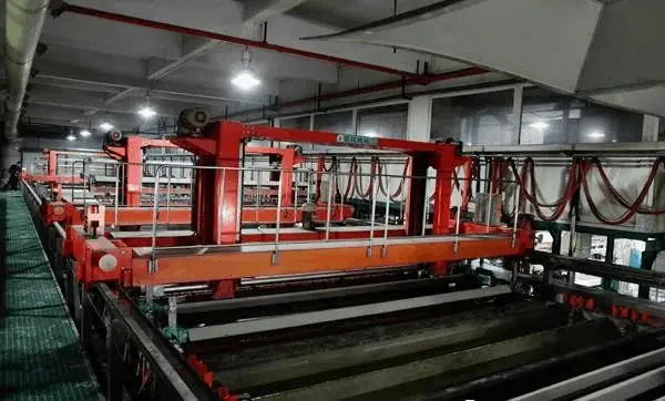
Equipment and Infrastructure Requirements
Basic Setup Components
- Plating tanks (PP or PVC lined)
- Filtration systems
- Temperature control units
- Rectifiers and power supplies
- Agitation mechanisms
Advanced Control Systems
| Control Parameter | Monitoring Method | Control Range |
| Bath Temperature | RTD sensors | ±1°C |
| pH Level | Online pH meters | ±0.1 units |
| Solution Level | Level sensors | ±5mm |
| Current Distribution | Hull cell analysis | Weekly check |
Environmental and Safety Considerations
Waste Treatment Requirements
| Waste Stream | Treatment Method | Disposal Criteria |
| Spent Solution | Ion exchange | <5 ppm Ni |
| Rinse Water | Reverse osmosis | pH 6-9 |
| Filter Cake | Stabilization | Landfill compatible |
Safety Protocols
- Personal protective equipment requirements
- Ventilation specifications
- Emergency response procedures
- Chemical handling guidelines
Quality Control and Testing
Testing Requirements
| Test Type | Frequency | Acceptance Criteria |
| Thickness | Every lot | ±10% of specification |
| Adhesion | Daily | No peeling at 90° bend |
| Surface Finish | Every shift | Ra ≤ 0.5 µm |
| Porosity | Weekly | Zero defects |
Documentation and Traceability
- Batch records
- Process control charts
- Equipment maintenance logs
- Operator training records
Cost Considerations
Operating Costs Breakdown
| Cost Component | Percentage of Total | Control Measures |
| Chemistry | 25-30% | Bath maintenance |
| Labor | 20-25% | Process automation |
| Energy | 15-20% | Efficiency optimization |
| Waste Treatment | 10-15% | Recovery systems |
| Maintenance | 10-15% | Preventive programs |
Process Optimization Strategies
Key Performance Indicators
| KPI | Target Range | Improvement Actions |
| First Pass Yield | >95% | Process control |
| Plating Rate | 0.5-1.0µm/min | Current optimization |
| Chemical Consumption | <10% variation | Bath analysis |
| Energy Efficiency | >80% | Equipment maintenance |
Future Trends and Developments
Emerging Technologies
- Pulse plating techniques
- Advanced brightener systems
- Automated process control
- Environmental-friendly alternatives
Frequently Asked Questions (FAQ)
Q1: What is the optimal thickness for nickel plating on PCB components?
A1: The optimal thickness typically ranges from 2 to 5 micrometers, depending on the application. Critical factors include the expected operating environment, mechanical stress requirements, and subsequent plating layers. For most commercial applications, 3 micrometers provides adequate protection and performance.
Q2: How can I prevent nickel plating adhesion failures?
A2: Adhesion failures can be prevented through proper surface preparation, including thorough cleaning, microetching, and acid activation. Maintaining optimal bath chemistry and ensuring proper current distribution are also critical. Regular Hull cell testing helps identify potential adhesion issues before they occur in production.
Q3: What are the main factors affecting nickel deposit stress?
A3: The primary factors affecting nickel deposit stress include:
- Bath temperature
- Current density
- pH level
- Brightener concentration
- Impurity levels Controlling these parameters within specified ranges helps minimize internal stress in the deposit.
Q4: How often should the plating bath be analyzed and maintained?
A4: Complete bath analysis should be performed weekly, with basic parameters (pH, temperature, specific gravity) checked daily. Brightener analysis should be conducted every shift, and carbon treatment should be performed monthly or as needed based on organic contamination levels.
Q5: What are the environmental considerations for nickel plating operations?
A5: Key environmental considerations include:
- Proper waste treatment and disposal
- Recovery and recycling of nickel from rinse waters
- Emission control through adequate ventilation
- Compliance with local environmental regulations
- Implementation of closed-loop recovery systems