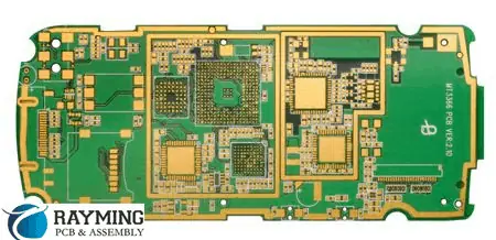
In the rapidly evolving world of electronics, High-Density Interconnect (HDI) Printed Circuit Boards (PCBs) have become crucial for meeting the demands of miniaturization and increased functionality. Among the challenges faced by PCB designers, Ball Grid Array (BGA) routing and impedance control stand out as critical aspects that significantly impact the performance and reliability of electronic devices. This article delves into the intricacies of BGA routing and impedance control in HDI PCBs, exploring best practices, challenges, and emerging technologies in this field.

Understanding BGA Technology
What is BGA?
Ball Grid Array (BGA) is a surface-mount packaging technology for integrated circuits. It is designed to address the increasing demand for higher pin counts and better electrical and thermal performance in a compact form factor.
Advantages of BGA
- Higher pin count in a smaller area
- Better thermal and electrical performance
- Reduced lead inductance
- Improved reliability due to self-alignment during reflow
Types of BGA Packages
| BGA Type | Description | Typical Application |
| Plastic BGA (PBGA) | Uses plastic substrate | Consumer electronics |
| Ceramic BGA (CBGA) | Uses ceramic substrate | High-reliability applications |
| Tape BGA (TBGA) | Uses polyimide tape substrate | Lightweight applications |
| Micro BGA (BGA) | Smaller pitch, typically < 0.8mm | Mobile devices |
| Flip Chip BGA (FCBGA) | Die is flipped and connected directly to substrate | High-performance computing |
HDI PCB Technology
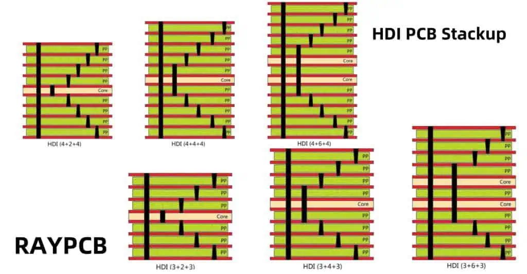
Definition of HDI
High-Density Interconnect (HDI) PCBs are characterized by higher wiring density per unit area. They typically feature finer lines and spaces, smaller vias and capture pads, and higher connection pad density than traditional PCBs.
Key Features of HDI PCBs
- Microvias (laser-drilled vias with diameter < 150µm)
- Fine line width and spacing (typically < 100µm)
- High layer count (often > 10 layers)
- Buried and blind vias
- Sequential lamination process
Benefits of HDI in BGA Routing
- Improved signal integrity
- Reduced board size and weight
- Enhanced electrical performance
- Better thermal management
- Increased design flexibility
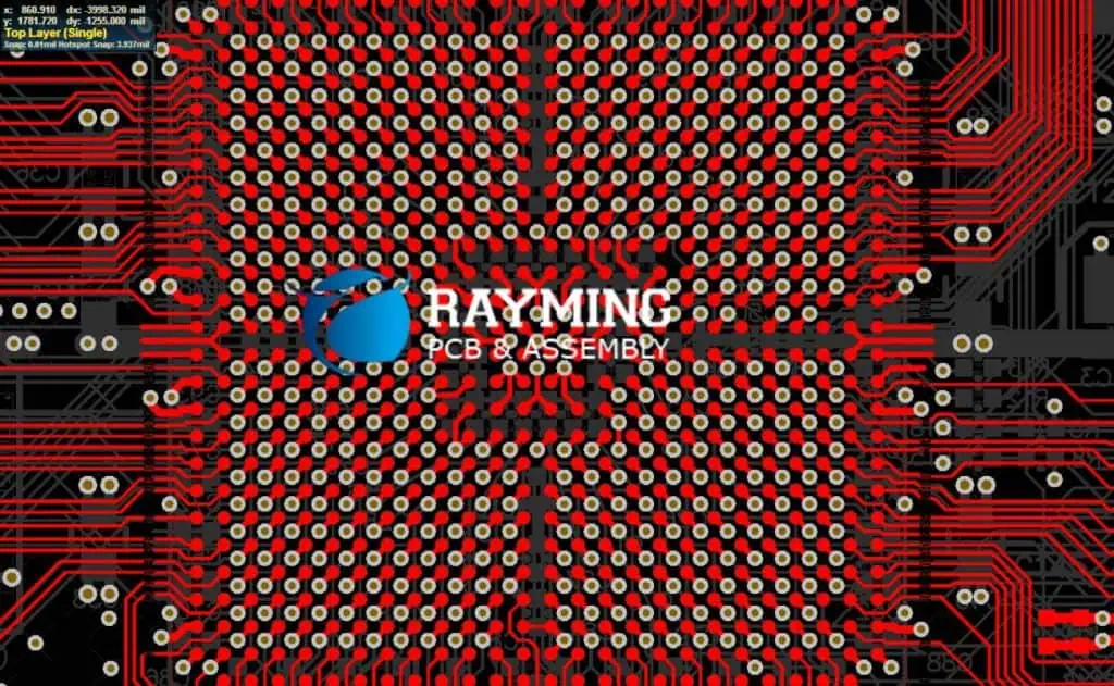
BGA Routing Strategies in HDI PCBs
Fanout Techniques
1. Dog Bone Fanout
- Description: Uses short traces (“dog bones”) to connect BGA pads to vias
- Pros: Simple, cost-effective
- Cons: Limited routing density, longer signal paths
2. Via-in-Pad
- Description: Vias placed directly in BGA pads
- Pros: Highest density, shortest signal paths
- Cons: More complex manufacturing, potential reliability issues
3. Via-near-Pad
- Description: Vias placed adjacent to BGA pads
- Pros: Balance between density and manufacturability
- Cons: Slightly longer signal paths than via-in-pad
Layer Stack-up Considerations
- Signal layer allocation
- Power and ground plane placement
- Microvia structure (stacked, staggered, or skip vias)
Routing Guidelines
- Maintain consistent trace widths
- Use 45-degree angles for direction changes
- Implement differential pair routing for high-speed signals
- Avoid routing under BGA to minimize crosstalk
- Consider signal grouping and length matching
Impedance Control in HDI PCBs
Importance of Impedance Control
Impedance control is crucial for maintaining signal integrity, especially in high-speed designs. It helps minimize signal reflections, reduce electromagnetic interference (EMI), and ensure proper signal transmission.
Factors Affecting Impedance
- Trace width
- Trace thickness
- Dielectric constant of PCB material
- Distance to reference planes
- Presence of nearby conductors
Common Impedance Values
| Application | Typical Impedance |
| Single-ended | 50Ω or 75Ω |
| Differential | 100Ω or 120Ω |
| USB | 90Ω differential |
| HDMI | 100Ω differential |
| PCIe | 100Ω differential |
Impedance Calculation
While exact impedance calculations can be complex, a simplified formula for microstrip impedance is:
Z₀ = 87 / √(εᵣ + 1.41) * ln(5.98h / (0.8w + t))
Where:
- Z₀ is the characteristic impedance
- εᵣ is the dielectric constant of the PCB material
- h is the height of the trace above the ground plane
- w is the width of the trace
- t is the thickness of the trace
Impedance Control Techniques
1. Controlled Dielectric Thickness
- Maintain consistent dielectric thickness between signal layers and adjacent planes
- Use high-quality, low-tolerance PCB materials
2. Trace Width Control
- Adjust trace widths to achieve desired impedance
- Use impedance calculators or field solvers for accurate calculations
3. Copper Weight Management
- Consider the impact of copper thickness on impedance
- Use consistent copper weights across the board
4. Reference Plane Design
- Ensure solid, uninterrupted reference planes
- Implement proper return path design
5. Differential Pair Routing
- Maintain consistent spacing between differential pairs
- Use serpentine routing for length matching
Challenges in BGA Routing and Impedance Control
1. High-Density Routing
- Limited space for routing between BGA pads
- Need for advanced PCB fabrication techniques
2. Signal Integrity
- Managing crosstalk and EMI in dense layouts
- Maintaining consistent impedance across the board
3. Thermal Management
- Dealing with heat dissipation in high-pin-count BGAs
- Balancing thermal and electrical requirements
4. Manufacturing Complexity
- Increased cost due to more complex fabrication processes
- Higher potential for manufacturing defects
5. Testing and Inspection
- Limited access to BGA solder joints for inspection
- Need for advanced testing techniques (e.g., X-ray inspection)
Advanced Techniques and Future Trends
1. 3D Routing
- Utilizing the Z-axis for more efficient routing
- Implementing embedded components
2. AI-Assisted Routing
- Using machine learning algorithms for optimal trace routing
- Automated impedance control and signal integrity analysis
3. Advanced Materials
- Development of low-loss, high-speed PCB materials
- Implementation of novel dielectrics for improved performance
4. Optical Interconnects
- Integration of optical layers in HDI PCBs
- Hybrid electro-optical routing solutions
5. Additive Manufacturing
- 3D-printed PCBs with integrated BGA routing
- Custom impedance control through additive processes
Best Practices for BGA Routing and Impedance Control
- Use appropriate design tools and simulators
- Implement a well-planned layer stack-up
- Follow manufacturer’s guidelines for BGA fanout
- Perform thorough signal integrity analysis
- Use controlled impedance techniques consistently
- Implement proper power distribution network (PDN) design
- Consider thermal management early in the design process
- Collaborate closely with PCB fabricators and assemblers
- Implement robust design for manufacturability (DFM) practices
- Conduct thorough testing and verification before production
Conclusion
BGA routing and impedance control in HDI PCBs represent critical challenges in modern electronic design. As devices continue to shrink in size while increasing in complexity and performance, mastering these aspects becomes essential for creating reliable, high-performance electronics.
The successful implementation of BGA routing and impedance control requires a deep understanding of PCB design principles, material properties, and manufacturing processes. Designers must balance the demands of high-density routing with the need for signal integrity, thermal management, and manufacturability.
As we look to the future, emerging technologies such as 3D routing, AI-assisted design, and advanced materials promise to push the boundaries of what’s possible in HDI PCB design. However, these advancements will also bring new challenges that designers must be prepared to address.
Ultimately, the key to success in BGA routing and impedance control lies in a holistic approach to PCB design, combining technical expertise with creativity and a willingness to embrace new technologies and methodologies. By following best practices and staying abreast of industry developments, designers can create HDI PCBs that meet the ever-increasing demands of modern electronics.
FAQ
Q1: What are the main advantages of using BGAs in HDI PCB designs?
A1: The main advantages of using BGAs in HDI PCB designs include:
- Higher pin count in a smaller area, allowing for more compact designs
- Improved electrical performance due to shorter interconnects and reduced parasitic effects
- Better thermal performance, as the entire bottom surface of the package can be used for heat dissipation
- Reduced lead inductance, which is crucial for high-speed applications
- Self-alignment during the reflow process, which can improve manufacturing yield
- More robust mechanical connection compared to leaded packages
- Ability to accommodate complex ICs with high I/O requirements
Q2: How does impedance control impact signal integrity in HDI PCBs?
A2: Impedance control significantly impacts signal integrity in HDI PCBs in several ways:
- Minimizes signal reflections: Consistent impedance along the signal path reduces reflections that can cause signal distortion.
- Reduces electromagnetic interference (EMI): Proper impedance control helps contain electromagnetic fields, reducing unwanted radiation and coupling.
- Improves signal quality: Controlled impedance environments maintain signal shape and timing, crucial for high-speed data transmission.
- Enhances power integrity: Well-controlled impedance in power distribution networks helps maintain stable power delivery to components.
- Enables faster edge rates: Consistent impedance allows for faster signal transition times without degradation.
- Facilitates matching: Controlled impedance makes it easier to match source, transmission line, and load impedances, maximizing power transfer.
- Supports higher bandwidth: By maintaining signal quality, impedance control enables higher data rates and bandwidth in digital systems.
Q3: What are the key challenges in routing high pin-count BGAs in HDI PCBs?
A3: Routing high pin-count BGAs in HDI PCBs presents several key challenges:
- Limited space: The high density of BGA pins leaves little room for routing between pads.
- Layer count management: Balancing the need for multiple routing layers with manufacturing constraints and cost considerations.
- Via management: Efficiently using and placing microvias to access inner layers without blocking too many routing channels.
- Signal integrity: Maintaining proper signal quality, especially for high-speed signals, in a dense routing environment.
- Power delivery: Ensuring adequate power and ground connections to all parts of the BGA.
- Thermal management: Dealing with heat dissipation in high-pin-count, densely routed areas.
- Manufacturability: Ensuring the design can be reliably manufactured and assembled despite its complexity.
- Impedance control: Maintaining consistent impedance in a constrained routing space.
- Crosstalk minimization: Managing electromagnetic coupling between closely spaced traces.
- Testability: Providing adequate test points and implementing design-for-test strategies in a limited-access environment.
Q4: How does the choice of PCB material affect impedance control in HDI designs?
A4: The choice of PCB material significantly affects impedance control in HDI designs in several ways:
- Dielectric constant: Materials with lower and more stable dielectric constants allow for more precise impedance control.
- Loss tangent: Lower loss tangent materials reduce signal attenuation, especially at high frequencies.
- Thickness control: Materials with tighter thickness tolerances enable more accurate impedance calculations and control.
- Thermal stability: Materials with lower coefficients of thermal expansion (CTE) maintain more consistent impedance across temperature ranges.
- Moisture absorption: Materials with lower moisture absorption rates maintain more stable electrical properties over time.
- Frequency dependence: Some materials maintain more consistent properties across a wide frequency range, crucial for broadband applications.
- Copper adhesion: Better copper adhesion allows for finer lines and spaces, enabling more precise impedance control.
- Homogeneity: More homogeneous materials provide more consistent electrical properties across the board.
- Cost: High-performance materials often come at a higher cost, requiring a balance between performance and budget.
Q5: What emerging technologies are likely to impact BGA routing and impedance control in the future?
A5: Several emerging technologies are poised to impact BGA routing and impedance control:
- 3D printing of PCBs: Enabling complex 3D routing strategies and custom impedance structures.
- AI-assisted routing: Using machine learning algorithms to optimize BGA breakout and routing patterns.
- Advanced PCB materials: Development of novel substrate materials with improved electrical and thermal properties.
- Embedded components: Integrating passive and active components within PCB layers to free up surface routing space.
- Optical interconnects: Incorporating optical layers in HDI PCBs for high-speed, low-loss signal transmission.
- Additive manufacturing techniques: Allowing for more precise control of trace geometries and material deposition.
- Advanced simulation tools: More accurate and efficient electromagnetic and thermal simulation capabilities.
- Photonic PCBs: Integration of optical waveguides with traditional PCB technology for ultra-high-speed applications.
- Flexible and stretchable electronics: New form factors requiring novel approaches to BGA mounting and impedance control.
- Quantum computing integration: Adapting PCB design for quantum computing requirements, including cryogenic operations and specialized signal routing.

