In today’s rapidly evolving electronics industry, ensuring the quality and reliability of complex components is paramount. One crucial aspect of this quality assurance process is BGA inspection. As Ball Grid Array (BGA) components become increasingly prevalent in modern electronic devices, mastering the art of BGA inspection has become essential for manufacturers and quality control professionals alike.
This comprehensive guide will delve into the intricacies of BGA inspection, exploring various methods, addressing common challenges, and providing practical solutions to ensure optimal results. Whether you’re new to the field or looking to refine your inspection techniques, this article will equip you with the knowledge and insights needed to excel in BGA inspection.
What is BGA Inspection?
Before we dive into the specifics of inspection methods and challenges, it’s crucial to understand what BGA inspection entails and why it’s so important in the electronics manufacturing process.
Defining BGA Inspection
BGA inspection refers to the process of examining and evaluating Ball Grid Array components to ensure proper installation, soldering quality, and overall integrity. BGAs are a type of surface-mount packaging used for integrated circuits, characterized by a grid of solder balls on the underside of the component that connect it to the printed circuit board (PCB).
The Challenge of Hidden Solder Joints
What makes BGA inspection particularly challenging is the nature of these connections. Unlike traditional through-hole or surface-mount components with visible leads, BGA solder joints are hidden beneath the component body. This concealment makes visual inspection difficult and necessitates specialized techniques and equipment for thorough evaluation.
The Critical Role of Inspection in Quality Assurance
BGA inspection plays a vital role in ensuring the reliability and performance of electronic devices. By identifying defects such as solder joint issues, misalignments, or internal damage, inspection helps prevent potential failures in the field. This process is essential for maintaining product quality, reducing warranty claims, and upholding a manufacturer’s reputation in the competitive electronics market.
Common Methods for BGA Inspection
To overcome the challenges posed by hidden solder joints, the industry has developed several inspection methods. Each technique offers unique advantages and limitations, often complementing one another in a comprehensive inspection strategy.
Visual Inspection
Overview of Manual Inspection Techniques
Visual inspection is the most basic and accessible method for BGA evaluation. It involves examining the component and surrounding area with the naked eye or using magnification tools such as loupes or microscopes.
Limitations for BGA Packages
While visual inspection can detect obvious issues like misalignment or excess solder, it’s severely limited when it comes to BGAs. The hidden nature of the solder joints means that many potential defects remain invisible to even the most trained eye.
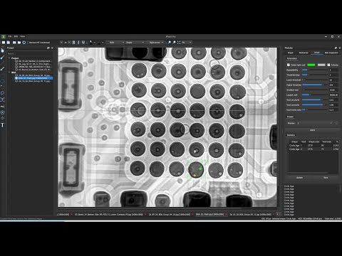
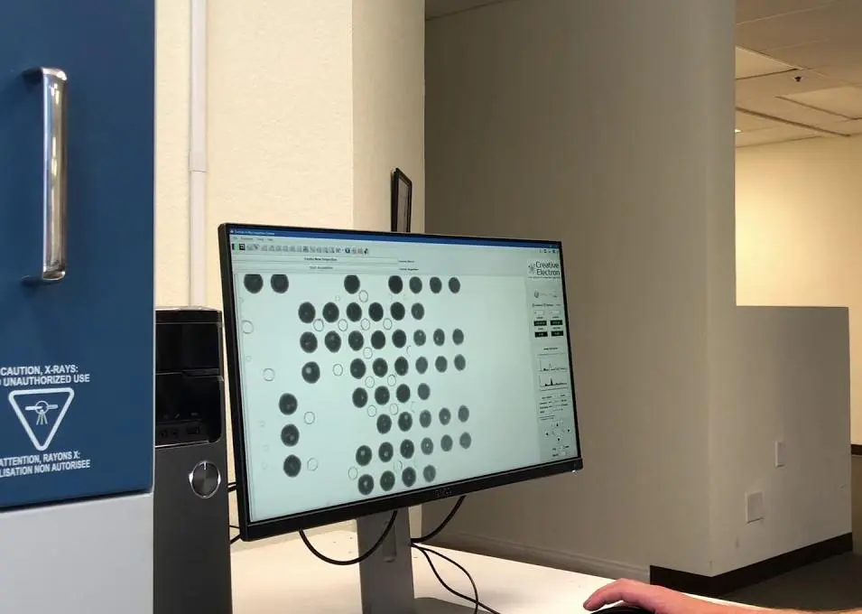
X-Ray Inspection
X-ray inspection has emerged as one of the most powerful tools for BGA evaluation, offering a non-destructive way to examine hidden solder joints.
How X-ray Machines Work for BGA Inspection
X-ray systems use high-energy electromagnetic radiation to penetrate the BGA package and PCB, creating a detailed image of the internal structures. Two main types of X-ray inspection are used:
- 2D X-ray: Provides a top-down view of the BGA, useful for detecting issues like bridging or missing solder balls.
- 3D Computed Tomography (CT): Offers a three-dimensional reconstruction of the BGA, allowing for more detailed analysis of solder joint shape and internal defects.
Advantages of X-ray Inspection
- Non-destructive: Allows for thorough inspection without damaging the component or PCB.
- Internal view: Provides clear images of hidden solder joints and internal structures.
- Versatility: Can detect a wide range of defects, from voids to misalignments.
Disadvantages of X-ray Inspection
- Cost: High-quality X-ray systems can be expensive, especially 3D CT machines.
- Skill requirement: Interpreting X-ray images accurately requires specialized training and experience.
- Time-consuming: Detailed analysis of complex BGAs can be time-intensive.
Automated Optical Inspection (AOI)
Automated Optical Inspection systems use high-resolution cameras and sophisticated algorithms to detect defects in electronic assemblies.
When and How AOI is Used for BGAs
AOI is primarily used for inspecting the visible aspects of BGA installation, such as:
- Component placement and alignment
- Solder paste deposition before reflow
- Post-reflow inspection of solder balls on the BGA perimeter
Limitations Due to Hidden Joints
While AOI is fast and efficient for many inspection tasks, its effectiveness for BGAs is limited by the inability to see beneath the component. It cannot directly inspect the critical solder joint connections, making it necessary to combine AOI with other inspection methods for comprehensive BGA evaluation.
Electrical Testing
Electrical testing methods provide a functional verification of BGA connections, complementing visual and X-ray inspection techniques.
Boundary Scan Testing (JTAG)
Joint Test Action Group (JTAG) boundary scan testing is a widely used method for verifying BGA connections electrically. This technique uses special circuitry built into the BGA and other components to test the integrity of connections without physical probing.
Pros and Cons for BGA Inspection
Pros:
- Can detect functional issues that may not be visible through other inspection methods
- Allows for testing of assembled PCBs without direct access to solder joints
- Automation-friendly, enabling high-volume testing
Cons:
- Requires BGAs and other components to be JTAG-compatible
- Cannot provide detailed information about the physical characteristics of solder joints
- May not detect all types of defects, such as minor voids or incipient cracks
Acoustic Microscopy
Acoustic microscopy is a specialized technique that uses high-frequency sound waves to examine the internal structure of BGAs and their solder joints.
Detecting Voids and Delamination in BGAs
By analyzing the reflection and transmission of sound waves through the BGA package and solder joints, acoustic microscopy can detect:
- Voids within solder joints
- Delamination between the BGA and PCB
- Cracks in the package or solder connections
This method is particularly useful for identifying defects that may not be visible through X-ray inspection, making it a valuable complementary technique in comprehensive BGA inspection strategies.
Microsectioning (Destructive Testing)
While non-destructive methods are preferred, there are instances where microsectioning becomes necessary for in-depth analysis of BGA solder joints.
When It’s Necessary and How It’s Performed
Microsectioning involves:
- Cutting through the BGA and PCB at specific points of interest
- Polishing the exposed cross-section
- Examining the solder joint structure under a microscope
This method is typically used:
- During failure analysis to determine the root cause of a defect
- For process validation and optimization
- In research and development of new BGA technologies
While destructive, microsectioning provides unparalleled detail about solder joint quality and can reveal issues that other inspection methods might miss.
Challenges in BGA Inspection
Despite the array of inspection methods available, BGA inspection remains a complex and challenging task. Understanding these challenges is crucial for developing effective inspection strategies.
Hidden Solder Joints
The fundamental challenge of BGA inspection lies in the hidden nature of the solder joints. This concealment makes it difficult to:
- Visually confirm proper soldering
- Detect subtle defects like partial connections or minor voids
- Assess the overall quality of the solder joint formation
Detecting Internal Defects
Identifying internal defects such as voids, cracks, and cold solder joints presents a significant challenge. These issues can seriously impact the reliability of the BGA connection but may not be immediately apparent through surface-level inspection.
Cost of Advanced Inspection Equipment
High-quality inspection equipment, particularly advanced X-ray and CT systems, represents a significant investment. This cost can be prohibitive for smaller manufacturers or those with lower production volumes, potentially limiting their ability to perform thorough BGA inspections.
Interpreting Complex Data
The sophisticated inspection methods used for BGAs often generate complex data sets. Interpreting this data accurately requires:
- Specialized training and experience
- Understanding of BGA manufacturing processes and potential defect types
- Ability to distinguish between true defects and benign anomalies
False Positives and Negatives
The complexity of BGA structures and the limitations of inspection methods can lead to:
- False positives: Incorrectly identifying a good joint as defective
- False negatives: Failing to detect an actual defect
Both scenarios can have significant consequences, either leading to unnecessary rework or allowing defective products to reach the market.
Read more about:
Solutions and Best Practices
Addressing the challenges of BGA inspection requires a multi-faceted approach combining technology, training, and strategic planning.
Investing in the Right Inspection Technology
Choosing appropriate inspection equipment is crucial. Consider:
- Production volume and complexity of BGAs used
- Types of defects most commonly encountered
- Budget constraints and return on investment
A mix of technologies (e.g., X-ray, AOI, and electrical testing) often provides the most comprehensive coverage.
Combining Multiple Inspection Methods
No single inspection method can detect all potential BGA defects. Implement a multi-stage inspection process that might include:
- AOI for initial alignment and visible defect check
- X-ray inspection for internal solder joint evaluation
- Electrical testing for functional verification
- Acoustic microscopy or destructive testing for in-depth analysis when necessary
Skilled Technician Training
Invest in comprehensive training programs for inspection personnel, covering:
- Principles of BGA technology and common defect types
- Operation of inspection equipment
- Interpretation of inspection data and images
- Understanding of manufacturing processes to identify root causes of defects
Design for Testability (DFT) in PCB Layout
Incorporate Design for Testability principles in PCB layout to facilitate easier and more effective BGA inspection:
- Include test points for electrical testing where possible
- Consider X-ray opacity when selecting PCB materials and components
- Optimize component placement for accessibility during inspection
Regular Calibration and Maintenance of Inspection Tools
Ensure the accuracy and reliability of inspection results by:
- Following manufacturer-recommended calibration schedules
- Performing regular maintenance on all inspection equipment
- Validating inspection processes periodically using known good and defective samples
Establishing Standard Inspection Protocols
Develop and implement standardized inspection procedures that:
- Define inspection criteria and acceptable quality levels
- Outline the sequence of inspection methods to be used
- Provide guidelines for interpreting and acting on inspection results
- Ensure consistency across different operators and production runs
Choosing the Right BGA Inspection Method for Your Needs
Selecting the most appropriate inspection methods depends on various factors specific to your manufacturing environment and product requirements.
Factors to Consider
When determining your BGA inspection strategy, evaluate:
- Production volume: High-volume production may require more automated solutions
- BGA complexity: More complex BGAs with finer pitch may need advanced inspection techniques
- Quality standards: Industry-specific or customer requirements may dictate inspection methods
- Budget constraints: Balance the cost of inspection equipment against the potential cost of field failures
- Typical defect types: Focus on methods that best detect your most common issues
Comparative Table: Method vs. Cost vs. Accuracy vs. Application
| Method | Cost | Accuracy | Best Application |
|---|---|---|---|
| Visual Inspection | Low | Low | Quick checks, obvious defects |
| X-ray (2D) | Medium-High | High | Solder joint integrity, voids |
| X-ray (3D CT) | Very High | Very High | Complex BGAs, detailed analysis |
| AOI | Medium | Medium | Component placement, visible defects |
| Electrical Testing | Medium | Medium-High | Functional verification |
| Acoustic Microscopy | High | High | Voids, delamination detection |
| Microsectioning | Medium | Very High | Failure analysis, process validation |
Conclusion
BGA inspection remains a critical aspect of electronics manufacturing, ensuring the reliability and performance of complex components in an increasingly miniaturized world. While the hidden nature of BGA solder joints presents significant challenges, a combination of advanced technologies, skilled personnel, and strategic methodologies can overcome these obstacles.
Remember that no single inspection method is perfect for all scenarios. The most effective approach often involves a carefully chosen combination of techniques, tailored to your specific manufacturing needs and quality requirements. By investing in the right tools, training your team effectively, and establishing robust inspection protocols, you can master the art of BGA inspection and maintain the highest standards of quality in your electronic products.
Continue to stay informed about advancements in BGA technology and inspection methods, as this field is constantly evolving. With dedication to continuous improvement and a commitment to quality, you can turn the challenge of BGA inspection into a competitive advantage in the electronics manufacturing industry.
FAQs About BGA Inspection
- What is the best method for BGA inspection? There is no single “best” method, as each technique has its strengths and limitations. A combination of methods, typically including X-ray inspection and electrical testing, often provides the most comprehensive results.
- How can I inspect BGA solder joints without damaging them? Non-destructive methods like X-ray inspection, acoustic microscopy, and electrical testing allow for thorough evaluation of BGA solder joints without causing damage.
- **What are common defects found during B