Introduction
The industrial battery charging sector is experiencing a significant transformation driven by the adoption of advanced semiconductor technologies. Silicon carbide (SiC) power switching devices have emerged as a game-changing solution, offering substantial advantages over traditional silicon-based components. These wide bandgap semiconductors enable faster switching speeds, superior low-loss operation, and increased power density without compromising performance reliability. The superior thermal properties and reduced switching losses of SiC technology have opened new possibilities for novel power factor correction topologies that were previously unattainable with conventional IGBT technology.
The evolution toward more efficient power conversion systems has become critical as industrial applications demand higher power densities, improved efficiency, and enhanced thermal management. Modern industrial chargers must meet stringent efficiency standards while providing reliable operation across diverse environmental conditions. This white paper provides a comprehensive analysis of various power topologies and presents detailed SiC MOSFET selection schemes for power factor correction (PFC) stages and primary power stages, alongside silicon-based MOSFET selection strategies for secondary synchronous rectification power stages.
Power Stage Architecture Overview
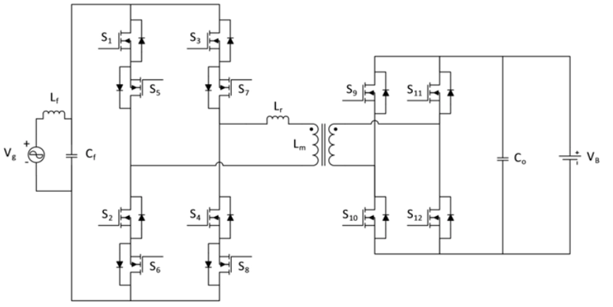
Industrial charger design requires careful consideration of power topology selection based on specific application requirements, including power levels, efficiency targets, thermal constraints, and cost considerations. The isolated DC-DC conversion stage represents a critical component in the overall system architecture, responsible for providing galvanic isolation between input and output while maintaining high efficiency across varying load conditions.
The selection of appropriate power topologies depends primarily on the target power level of the application. Different topologies offer distinct advantages in terms of component stress, magnetic utilization, control complexity, and overall system efficiency. Understanding these trade-offs is essential for optimal system design and component selection.
Half-Bridge LLC Topology
Applications and Power Ranges
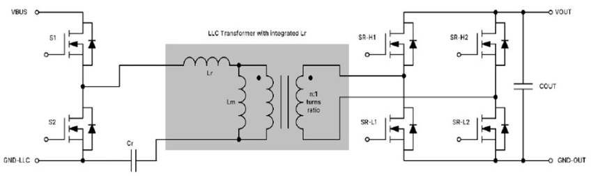
The half-bridge LLC topology with full-bridge synchronous rectification on the secondary side represents an excellent solution for mid-range charger applications spanning from 600W to 3.0kW. This topology has gained widespread acceptance due to its inherent advantages, including zero-voltage switching (ZVS) operation, reduced electromagnetic interference (EMI), and excellent load regulation characteristics.
For lower power applications ranging from 600W to 1.0kW, gallium nitride (GaN) power switches offer optimal performance due to their superior switching characteristics and reduced gate charge requirements. The high electron mobility and low on-resistance of GaN devices make them particularly well-suited for high-frequency operation, enabling compact magnetic designs and reduced system size.
For higher power applications in the 1.2kW to 3.0kW range, SiC MOSFETs become the preferred choice. The superior thermal conductivity and higher current handling capability of SiC devices enable efficient operation at these power levels while maintaining acceptable junction temperatures and long-term reliability.
Component Selection and Implementation
The primary-side half-bridge circuit benefits significantly from the implementation of high-performance SiC MOSFETs. The NTH4L045N065SC1 and NTBL032N065M3S 650V EliteSiC MOSFETs represent optimal choices for this application. These devices feature low on-resistance, fast switching characteristics, and robust avalanche energy ratings, making them ideal for resonant converter applications where devices must handle varying voltage and current stresses.
For secondary-side synchronous rectification, silicon MOSFETs in the 80–150V range provide the best balance of performance and cost-effectiveness. The selection of secondary-side devices must consider the specific output voltage requirements of the target application. For 48V battery charger applications, the NTBLS0D8N08X silicon MOSFET offers excellent performance with low conduction losses and fast switching capabilities. For higher voltage applications targeting 80V–120V battery systems, the NTBLS4D0N15MC silicon MOSFET provides optimal performance characteristics.
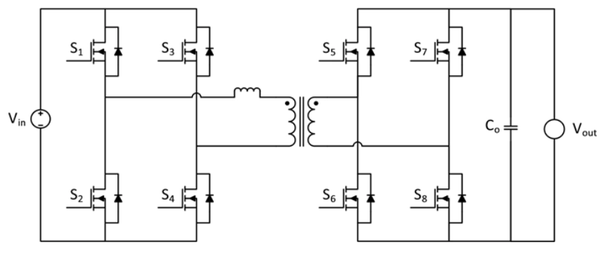
Full-Bridge LLC Topology
Configuration and Operating Principles
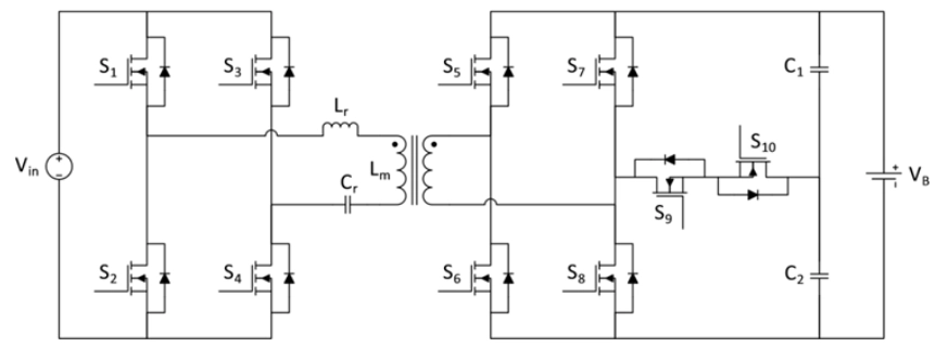
The full-bridge LLC topology extends the power handling capability of the basic half-bridge configuration by employing two half-bridges (S1–S2 and S3–S4) on the primary side. This configuration includes the transformer’s primary winding inductance (Lm) and the resonant LC network, providing enhanced power delivery capability and improved magnetic utilization.
The operational strategy involves driving diagonally arranged SiC MOSFETs in the full-bridge circuit with identical gate signals, ensuring proper switching sequence and minimizing cross-conduction risks. This approach simplifies the gate drive circuitry while maintaining optimal switching performance.
Secondary-Side Implementation
The secondary-side full-bridge LLC topology incorporates two half-bridges (S5–S6 and S7–S8) utilizing high-performance synchronous rectification silicon MOSFETs. The integration of bidirectional silicon MOSFET switches (S9–S10) enables voltage multiplication functionality, providing a wide output voltage range capability spanning 40V to 120V.
This wide voltage range capability makes the topology particularly suitable for universal battery charger applications that must accommodate various battery chemistries and voltage specifications. The bidirectional switches provide additional control flexibility, enabling precise output voltage regulation across the entire operating range.
Multi-Transformer Configurations
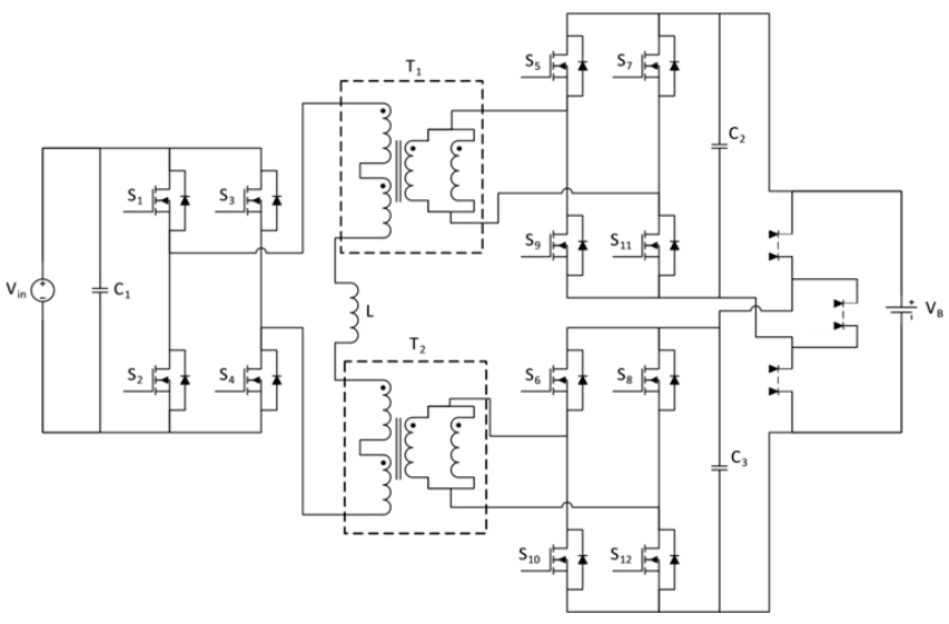
For applications requiring power levels between 4.0kW and 6.6kW, a full-bridge LLC topology with dual transformers and two secondary-side full-bridge synchronous rectification circuits provides optimal performance. This configuration distributes power losses across multiple magnetic components, improving thermal management and system reliability while maintaining high efficiency operation.
Interleaved Three-Phase LLC Topology
High-Power Applications
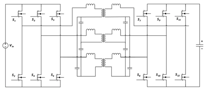
The interleaved three-phase LLC topology addresses the requirements of high-power applications ranging from 6.6kW to 12.0kW. This advanced configuration distributes power losses across multiple switches and transformers, significantly improving thermal management and enabling higher power density designs.
The topology consists of three half-bridges (S1–S2, S3–S4, and S5–S6) on the primary side, each associated with dedicated resonant LC circuits and transformers with specific magnetizing inductance values. The secondary side features three corresponding half-bridges (S7–S8, S9–S10, and S11–S12) with resonant LC networks optimized for bidirectional operation capability.
Phase Management and Ripple Reduction
The three primary-side half-bridges operate at the resonant switching frequency with a precisely controlled 120-degree phase difference between each phase. This phase management strategy produces output ripple at three times the fundamental switching frequency, dramatically reducing the required size of output filter capacitors and improving overall system response characteristics.
The reduced ripple current also decreases stress on output capacitors, extending their operational lifetime and improving system reliability. The interleaved operation provides inherent redundancy, allowing continued operation even if one phase experiences a fault condition.
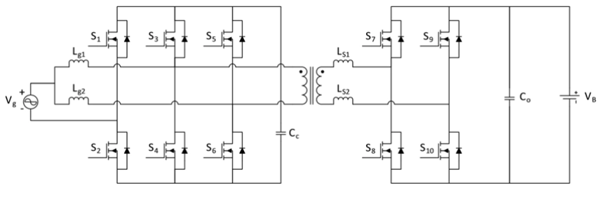
Dual Active Bridge (DAB) Topology
High-Power Industrial Applications
The dual active bridge topology represents the optimal solution for high-power industrial charger applications, particularly those used in heavy-duty equipment such as ride-on lawn mowers, industrial forklifts, and electric motorcycles. The DAB topology excels in applications requiring power levels from 6.6kW to 11.0kW, offering excellent bidirectional power flow capability and robust performance characteristics.
Single-Stage Implementation
For industrial applications with 120–347V single-phase AC input requirements, a single-stage topology approach provides significant advantages in terms of component count reduction and improved power conversion efficiency. The dual active bridge with bidirectional AC switches on the primary side offers exceptional performance for industrial charger applications spanning 4.0kW to 11.0kW power levels.
Component Selection for DAB Applications
The implementation of bidirectional switches in DAB applications requires careful consideration of semiconductor technology selection. Both 650–750V SiC MOSFETs and GaN HEMTs provide suitable performance characteristics for bidirectional switch applications. The NTBL032N065M3S and NTBL023N065M3S 650V M3S EliteSiC MOSFETs are specifically recommended for primary-side bidirectional switch implementations.
These devices can be effectively implemented by integrating two dies into industry-standard TOLL (TO-Leadless) or TOLT (TO-Leadless Top-cooled) packages, providing compact solutions with excellent thermal performance. GaN technology also presents viable alternatives for bidirectional switch applications, particularly where high switching frequency operation is required.
Advanced Integrated Topologies
Interleaved Totem-Pole PFC Integration
An noteworthy advancement in single-stage topology design involves the integration of interleaved totem-pole PFC with full-bridge isolated LLC DC-DC conversion. This innovative approach combines the benefits of active PFC correction with efficient isolated DC-DC conversion in a single-stage implementation.
The integrated topology reduces component count, improves power factor correction performance, and enhances overall system efficiency. The interleaved operation provides excellent input current ripple cancellation while the LLC section ensures optimal isolated power transfer with minimal switching losses.
Conclusion and Future Trends
The selection of appropriate isolated DC-DC power stages for industrial chargers requires comprehensive understanding of application requirements, power level specifications, and component characteristics. SiC technology continues to drive innovation in power conversion systems, enabling higher efficiency, increased power density, and enhanced thermal performance.
The introduction of onsemi’s 650V M3S EliteSiC MOSFET family represents a significant advancement in wide bandgap semiconductor technology, offering superior performance characteristics for demanding industrial applications. As battery technology continues to evolve and power requirements increase, the importance of optimal power stage selection will continue to grow.
Future developments in wide bandgap semiconductors, including improved SiC and GaN technologies, will further expand the possibilities for efficient, compact, and reliable industrial charger designs. The ongoing evolution toward electrification across industrial sectors ensures that advanced power conversion technologies will remain critical enablers for next-generation applications.