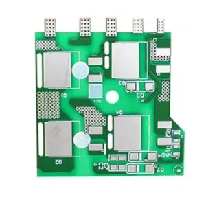
Printed Circuit Boards (PCBs) are the backbone of modern electronics, providing the necessary platform for electrical connections and mechanical support for electronic components. As technology advances, the demand for more efficient, reliable, and miniaturized PCBs has grown significantly. One of the emerging solutions to meet these demands is the Thin Film Ceramic PCB. This type of PCB is gaining traction in various high-performance applications due to its unique properties and advantages over traditional PCB materials. In this article, we will explore what Thin Film Ceramic PCBs are, their manufacturing process, key characteristics, applications, and the benefits they offer.
What is a Thin Film Ceramic PCB?
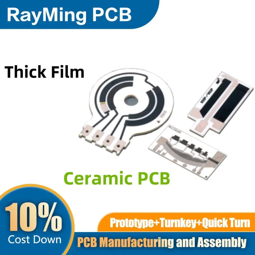
A Thin Film Ceramic PCB is a type of printed circuit board that uses a ceramic substrate, typically made from materials like aluminum oxide (Al2O3), aluminum nitride (AlN), or beryllium oxide (BeO), combined with thin-film deposition techniques to create conductive traces and other circuit elements. Unlike conventional PCBs that use organic materials like FR-4 (a glass-reinforced epoxy laminate), Thin Film Ceramic PCBs leverage the superior thermal, electrical, and mechanical properties of ceramics.
The “thin film” aspect refers to the deposition of conductive and insulating layers on the ceramic substrate using advanced techniques such as sputtering, evaporation, or chemical vapor deposition (CVD). These layers are extremely thin, often in the range of nanometers to micrometers, allowing for high precision and miniaturization in circuit design.


Manufacturing Process of Thin Film Ceramic PCBs
The manufacturing process of Thin Film Ceramic PCBs is highly specialized and involves several key steps:
- Substrate Preparation: The process begins with the selection of a ceramic substrate. The substrate is cleaned and polished to ensure a smooth surface, which is crucial for the subsequent deposition of thin films.
- Thin Film Deposition: Conductive materials such as gold, silver, copper, or aluminum are deposited onto the ceramic substrate using techniques like sputtering or evaporation. These materials form the conductive traces, pads, and other circuit elements. Insulating layers may also be deposited to create multi-layer circuits or to protect certain areas of the board.
- Patterning: Photolithography is commonly used to pattern the thin films. A photoresist is applied to the substrate, exposed to UV light through a mask, and then developed to create the desired circuit pattern. The exposed areas are then etched away, leaving behind the conductive traces.
- Annealing: After patterning, the PCB may undergo an annealing process to improve the adhesion of the thin films to the ceramic substrate and to enhance the electrical properties of the conductive traces.
- Component Assembly: Once the thin film layers are in place, electronic components are mounted onto the PCB using surface-mount technology (SMT) or other assembly techniques. The components are then soldered to the conductive pads.
- Testing and Inspection: The final step involves rigorous testing and inspection to ensure the PCB meets the required electrical and mechanical specifications. This may include electrical continuity tests, thermal cycling, and visual inspections.
Key Characteristics of Thin Film Ceramic PCBs
Thin Film Ceramic PCBs exhibit several unique characteristics that make them suitable for high-performance applications:
- High Thermal Conductivity: Ceramic materials like aluminum nitride (AlN) and beryllium oxide (BeO) have excellent thermal conductivity, allowing for efficient heat dissipation. This is particularly important in high-power applications where heat management is critical.
- Low Thermal Expansion: Ceramics have a low coefficient of thermal expansion (CTE), which means they expand and contract less with temperature changes compared to organic materials. This property reduces the risk of thermal stress and improves the reliability of the PCB, especially in environments with fluctuating temperatures.
- Excellent Electrical Insulation: Ceramic substrates provide superior electrical insulation, reducing the risk of short circuits and improving the overall performance of the PCB.
- High Precision and Miniaturization: The thin-film deposition process allows for extremely fine traces and small feature sizes, enabling the creation of highly compact and complex circuits. This is particularly beneficial in applications where space is at a premium, such as in medical devices or aerospace electronics.
- Chemical and Mechanical Stability: Ceramics are chemically inert and mechanically robust, making Thin Film Ceramic PCBs resistant to corrosion, wear, and environmental degradation. This enhances the longevity and reliability of the PCB in harsh operating conditions.
Applications of Thin Film Ceramic PCBs
Thin Film Ceramic PCBs are used in a wide range of applications where high performance, reliability, and miniaturization are required. Some of the key application areas include:
- Aerospace and Defense: The aerospace and defense industries demand electronics that can withstand extreme temperatures, vibrations, and radiation. Thin Film Ceramic PCBs are ideal for these applications due to their thermal stability, mechanical strength, and resistance to environmental stressors.
- Medical Devices: In medical electronics, such as implantable devices and diagnostic equipment, reliability and precision are paramount. Thin Film Ceramic PCBs offer the necessary performance and miniaturization to meet the stringent requirements of medical applications.
- High-Power Electronics: Power electronics, such as inverters, converters, and motor drives, generate significant heat and require efficient thermal management. Thin Film Ceramic PCBs, with their high thermal conductivity, are well-suited for these applications.
- Telecommunications: The telecommunications industry relies on high-frequency and high-speed electronics, where signal integrity and minimal loss are critical. Thin Film Ceramic PCBs provide the necessary electrical performance and stability for these demanding applications.
- Automotive Electronics: With the increasing electrification of vehicles, automotive electronics require PCBs that can operate reliably under high temperatures and harsh conditions. Thin Film Ceramic PCBs are increasingly being used in electric vehicles (EVs) and advanced driver-assistance systems (ADAS).
- LED Lighting: High-power LED lighting systems generate significant heat, and efficient thermal management is essential to maintain performance and longevity. Thin Film Ceramic PCBs are commonly used in LED modules to ensure effective heat dissipation.
Read more about:
Advantages of Thin Film Ceramic PCBs
Thin Film Ceramic PCBs offer several advantages over traditional PCBs, making them a preferred choice for high-performance applications:
- Superior Thermal Management: The high thermal conductivity of ceramic substrates allows for efficient heat dissipation, reducing the risk of overheating and improving the reliability of electronic components.
- Enhanced Reliability: The low thermal expansion and chemical stability of ceramics contribute to the long-term reliability of Thin Film Ceramic PCBs, even in harsh environments.
- Miniaturization: The ability to create fine traces and small feature sizes enables the design of compact and lightweight PCBs, which is essential for applications where space is limited.
- High-Frequency Performance: Thin Film Ceramic PCBs exhibit excellent electrical properties, including low dielectric loss and high signal integrity, making them suitable for high-frequency and high-speed applications.
- Durability: Ceramic materials are inherently durable and resistant to wear, corrosion, and environmental degradation, ensuring the longevity of the PCB.
Challenges and Considerations
Despite their numerous advantages, Thin Film Ceramic PCBs also present some challenges:
- Cost: The manufacturing process for Thin Film Ceramic PCBs is more complex and expensive compared to traditional PCBs. The cost of ceramic substrates and the specialized equipment required for thin-film deposition contribute to the higher price.
- Fragility: While ceramics are mechanically robust, they can be brittle and prone to cracking under mechanical stress. Care must be taken during handling and assembly to avoid damage.
- Limited Flexibility: Unlike flexible PCBs, Thin Film Ceramic PCBs are rigid and cannot be bent or flexed. This limits their use in applications where flexibility is required.
Conclusion
Thin Film Ceramic PCBs represent a significant advancement in PCB technology, offering superior thermal management, reliability, and miniaturization compared to traditional PCBs. Their unique properties make them ideal for high-performance applications in industries such as aerospace, medical devices, telecommunications, and automotive electronics. While they come with higher costs and some limitations, the benefits they offer in terms of performance and durability make them a valuable solution for demanding electronic applications. As technology continues to evolve, Thin Film Ceramic PCBs are likely to play an increasingly important role in the development of next-generation electronics.