“We’ve trusted Rayming with multiple PCB orders, and they’ve never disappointed. Their manufacturing process is top-tier, and their team is always helpful. A+ service!”
Rayming provides top-notch PCB assembly services at competitive prices. Their customer support is excellent, and they always go the extra mile to ensure satisfaction. A trusted partner!
The increasing demand for miniaturization in electronic devices has led to the widespread adoption of 0201 components and microBall Grid Array (BGA) packages. Understanding and managing PCB tolerances for these ultra-small components is crucial for successful assembly and reliable product performance. This comprehensive guide explores the critical aspects of PCB design, manufacturing tolerances, and best practices for working with 0201 components and micro BGAs.
Understanding 0201 Components
Dimensional Specifications
0201 components represent one of the smallest surface mount device (SMD) form factors available in mass production. The designation “0201” refers to the imperial measurements:
Dimension
Imperial (inches)
Metric (mm)
Length
0.024 ± 0.002
0.60 ± 0.05
Width
0.012 ± 0.001
0.30 ± 0.03
Height
0.006 ± 0.001
0.15 ± 0.03
Terminal
0.008 ± 0.001
0.20 ± 0.03
Critical Tolerance Considerations
Pad Design Parameters
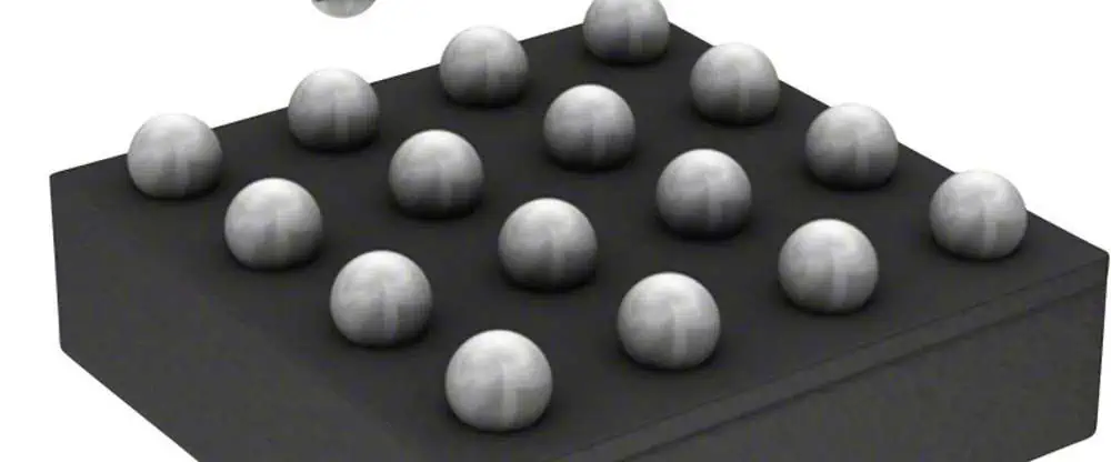
DSBGA
The pad design for 0201 components requires precise control of several key parameters:
Q1: What is the minimum recommended trace width for routing under micro BGAs?
A1: The minimum recommended trace width for routing under micro BGAs is 0.075mm (3 mils). However, it’s important to consider manufacturing capabilities and impedance requirements when selecting final trace dimensions.
Q2: How does moisture sensitivity affect micro BGA assembly?
A2: Moisture sensitivity can lead to package cracking during reflow if proper handling procedures aren’t followed. Components should be stored in moisture barrier bags with desiccant and humidity indicators, and floor life limitations must be strictly observed based on the MSL level.
Q3: What are the key considerations for selecting PCB surface finish for 0201 and micro BGA applications?
A3: ENIG or ENEPIG are preferred surface finishes due to their excellent planarity, solderability, and shelf life. These finishes provide consistent solderability and help prevent oxidation issues during assembly.
Q4: How can void percentage in micro BGA solder joints be minimized?
A4: Void percentage can be minimized through proper reflow profile optimization, using quality solder paste, implementing appropriate pad designs, and ensuring proper storage and handling of components and materials.
Q5: What are the recommended inspection methods for 0201 components and micro BGAs?
A5: A combination of AOI, X-ray inspection, and SPI (Solder Paste Inspection) is recommended. AOI can verify component placement and presence, X-ray inspection can check solder joint quality and void content, while SPI ensures proper solder paste deposit volume and position.
Conclusion
Successfully implementing 0201 components and micro BGAs requires careful attention to PCB design tolerances, manufacturing processes, and quality control measures. By following the guidelines and specifications outlined in this document, engineers can achieve reliable and consistent assembly results. Regular review and updates of these parameters based on production feedback and new technology developments will help maintain high-quality standards in electronic assembly.