Printed Circuit Board (PCB) design is a critical aspect of electronic product development. One of the key factors that contribute to the overall efficiency, reliability, and manufacturability of a PCB is the orientation of its components. Proper component orientation can significantly impact the board’s performance, assembly process, and long-term reliability. This article delves into the importance of optimizing PCB component orientation and provides comprehensive guidelines for engineers and designers to achieve the best results.

The Importance of Component Orientation
Electrical Performance
Component orientation plays a crucial role in the electrical performance of a PCB. Proper orientation can:
- Minimize signal interference
- Reduce electromagnetic emissions
- Improve signal integrity
- Enhance overall circuit efficiency
Thermal Management
The orientation of components affects heat dissipation and thermal management on the PCB. Optimal orientation can:
- Facilitate better heat distribution
- Prevent hotspots
- Improve overall thermal performance
Manufacturing and Assembly
Correct component orientation is essential for efficient manufacturing and assembly processes. It can:
- Streamline automated assembly
- Reduce assembly errors
- Improve soldering quality
- Enhance overall production yield
Reliability and Longevity
Proper orientation contributes to the long-term reliability of the PCB by:
- Reducing mechanical stress on components
- Minimizing the risk of component failure
- Improving resistance to environmental factors
Guidelines for Optimizing Component Orientation
1. Follow Industry Standards and Best Practices
IPC Standards
Adhere to IPC (Institute of Printed Circuits) standards for component placement and orientation. Key standards include:
- IPC-7351B: Generic Requirements for Surface Mount Design and Land Pattern Standard
- IPC-2221: Generic Standard on Printed Board Design
- IPC-2222: Sectional Design Standard for Rigid Organic Printed Boards
Manufacturer Guidelines
Consider component manufacturer guidelines for optimal orientation and placement.
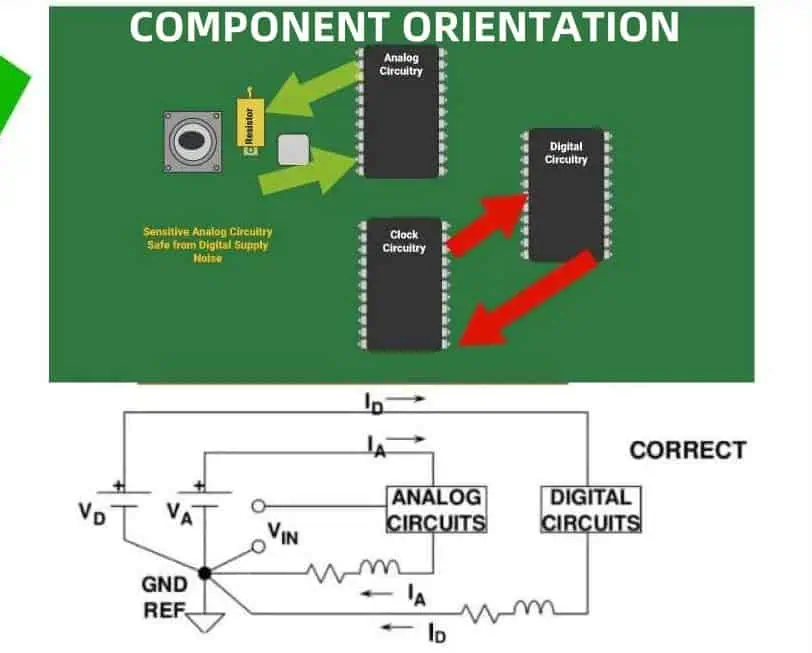
2. Prioritize Signal Integrity
Component Placement
- Place sensitive components away from noise sources
- Group related components together
- Minimize signal path lengths
Orientation for Signal Flow
- Align components to facilitate logical signal flow
- Orient components to minimize crossovers and vias
3. Optimize for Thermal Management
Heat-Generating Components
- Orient high-power components for optimal heat dissipation
- Align components to create thermal corridors
Thermal Considerations
- Consider airflow direction when orienting components
- Use thermal simulations to validate component orientation
4. Enhance Manufacturing and Assembly Efficiency
Pick-and-Place Optimization
- Orient components consistently for efficient pick-and-place operations
- Align component reference designators for easy identification
Soldering Considerations
- Orient components to facilitate proper solder fillets
- Consider reflow direction when orienting surface-mount components
5. Improve Testability and Maintenance
Test Point Access
- Orient components to allow easy access to test points
- Consider in-circuit test (ICT) requirements when placing components
Rework and Repair
- Orient components to facilitate easy rework and replacement
- Consider clearance for soldering tools and equipment
Component-Specific Orientation Guidelines
Integrated Circuits (ICs)
- Align pin 1 consistently across the board (e.g., top-left corner)
- Orient ICs to minimize crossing of critical signals
Capacitors and Resistors
- Orient passive components in the same direction when possible
- Align components parallel or perpendicular to the board edge
Inductors and Transformers
- Orient magnetic components to minimize electromagnetic interference (EMI)
- Consider mutual inductance effects when placing multiple inductors
Connectors
- Orient connectors for easy access and cable management
- Align connectors with board edges when appropriate
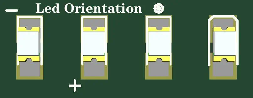
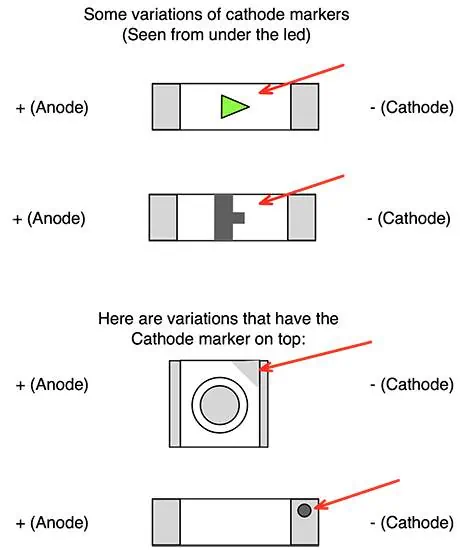
LEDs and Optical Components
- Orient LEDs consistently for uniform light distribution
- Consider viewing angles when placing optical components
Advanced Techniques for Component Orientation Optimization
1. Design for Manufacturing (DFM) Analysis
Utilize DFM software tools to:
- Identify potential manufacturing issues related to component orientation
- Optimize component placement for assembly efficiency
- Validate compliance with design rules and standards
2. Signal Integrity Simulation
Employ signal integrity simulation tools to:
- Analyze the impact of component orientation on signal quality
- Optimize critical signal paths
- Identify and mitigate potential EMI issues
3. Thermal Analysis and Simulation
Use thermal analysis software to:
- Evaluate the effect of component orientation on heat distribution
- Identify potential hotspots
- Optimize component placement for improved thermal performance
4. 3D Modeling and Visualization
Leverage 3D PCB design tools to:
- Visualize component orientation in a three-dimensional space
- Identify potential mechanical conflicts
- Optimize component placement for space utilization
5. Machine Learning and AI-Assisted Placement
Explore emerging technologies that use machine learning and artificial intelligence to:
- Suggest optimal component orientations based on design goals
- Analyze large datasets of successful PCB designs for pattern recognition
- Continuously improve placement strategies based on manufacturing feedback
Case Studies: Successful Component Orientation Strategies
Case Study 1: High-Speed Digital Design
| Aspect | Strategy | Result |
| Signal Integrity | Aligned critical components along signal paths | 30% reduction in signal reflections |
| EMI Reduction | Oriented ICs to minimize loop areas | 25% decrease in electromagnetic emissions |
| Thermal Management | Created thermal corridors for heat dissipation | 15% improvement in overall thermal performance |
Case Study 2: Power Supply Design
| Aspect | Strategy | Result |
| Efficiency | Optimized placement of power components | 10% increase in power conversion efficiency |
| Thermal Performance | Oriented heat-generating components for better airflow | 20% reduction in maximum component temperature |
| EMI Suppression | Aligned filter components to minimize noise coupling | 40% reduction in conducted emissions |
Case Study 3: IoT Device Miniaturization
| Aspect | Strategy | Result |
| Space Utilization | Optimized component orientation for compact layout | 25% reduction in overall PCB size |
| Assembly Efficiency | Standardized component orientations | 15% decrease in assembly time |
| Antenna Performance | Carefully oriented RF components | 20% improvement in wireless range |
Common Pitfalls and How to Avoid Them
- Inconsistent orientation of similar components
- Solution: Establish and follow standardized orientation guidelines
- Neglecting thermal considerations in component placement
- Solution: Conduct thermal simulations and prioritize heat dissipation in layout
- Poor accessibility for testing and rework
- Solution: Consider test point access and rework requirements during initial placement
- Ignoring manufacturability in component orientation
- Solution: Collaborate with PCB manufacturers and consider their feedback
- Overlooking signal integrity in high-speed designs
- Solution: Use signal integrity simulations to validate component orientations
Future Trends in PCB Component Orientation
- Increased adoption of AI-assisted placement and routing
- Integration of augmented reality (AR) in PCB design processes
- Advanced thermal management techniques for high-density designs
- Enhanced focus on design for recycling and sustainability
- Automation of compliance checks for component orientation standards
Conclusion
Optimizing PCB component orientation is a critical aspect of successful electronic design. By following industry standards, considering electrical and thermal performance, and prioritizing manufacturability, designers can create more efficient, reliable, and cost-effective PCBs. As technology continues to advance, new tools and techniques will emerge to further enhance the component orientation process, leading to even more innovative and high-performing electronic products.
Frequently Asked Questions (FAQ)
Q1: How does component orientation affect PCB manufacturing costs?
A1: Proper component orientation can significantly reduce manufacturing costs by:
- Streamlining the assembly process, reducing production time
- Minimizing errors during automated pick-and-place operations
- Improving soldering quality, reducing rework and scrap rates
- Enhancing overall production yield
Q2: What are the key considerations for orienting components in high-frequency PCB designs?
A2: In high-frequency PCB designs, consider the following:
- Minimize signal path lengths to reduce signal degradation
- Orient components to reduce loop areas and minimize EMI
- Align sensitive components to avoid coupling and crosstalk
- Consider the impact of component orientation on impedance matching
Q3: How can I ensure consistent component orientation across multiple PCB designs?
A3: To maintain consistency across designs:
- Develop and document standardized orientation guidelines for your organization
- Create component libraries with predefined orientations
- Use design rule checks (DRCs) to enforce orientation standards
- Conduct regular design reviews to ensure compliance with guidelines
Q4: What tools can help optimize component orientation in PCB design?
A4: Several tools can assist in optimizing component orientation:
- PCB design software with advanced placement and routing capabilities
- Signal integrity simulation tools
- Thermal analysis software
- Design for Manufacturing (DFM) analysis tools
- 3D PCB visualization software
Q5: How does component orientation impact the reliability of a PCB in harsh environments?
A5: Proper component orientation can enhance PCB reliability in harsh environments by:
- Improving heat dissipation, reducing thermal stress on components
- Minimizing mechanical stress on solder joints during vibration or thermal cycling
- Enhancing resistance to moisture ingress and corrosion
- Facilitating better conformal coating coverage for environmental protection