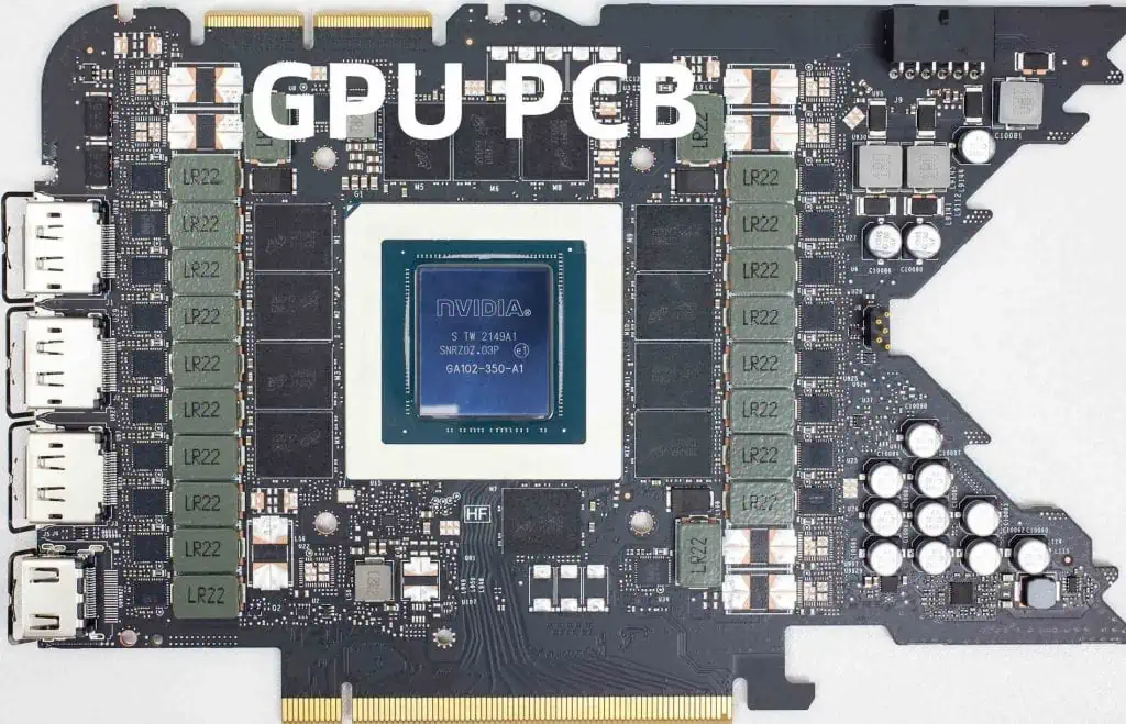
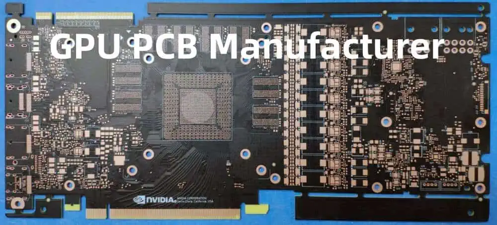
A PCB (Printed Circuit Board) is an integral component of all computer graphics cards, including GPUs (Graphics Processing Units). The PCB serves several key functions:
Mounting Components
The PCB provides a surface to mount and connect critical GPU components like:
- GPU chip
- Memory chips
- Power circuitry
- Connectors
- Support chips
Facilitating Communication
The traces etched into the PCB facilitate communication between mounted components. This allows the GPU chip to send and receive data from memory chips and other components.
Power Delivery
The PCB contains carefully designed power circuitry to provide stable, clean power to GPU components. This includes voltage regulator modules (VRMs).
Structural Integrity
The PCB gives the graphics card physical structure and integrity for handling and installation. Materials like FR4 fiberglass are common.
PCB Design Considerations for GPUs
Designing a GPU PCB requires careful planning for:
Signal Integrity
Trace paths must maintain signal integrity at high GPU clock speeds (often 1GHz+). This requires impedance tuning and careful routing.
Power Integrity
With GPUs consuming 100W+, the PCB must provide ample power with minimal ripple and noise. This demands quality VRMs and capacitors.
Thermal Dissipation
The PCB must dissipate substantial heat from the GPU chip and power circuitry. This requires thermal pads, heat pipes, and airflow-optimized board shapes.
Component Placement
Component placement impacts many attributes like signal routing, heat levels in specific areas, etc. Optimization is a complex balance.
EMI Reduction
Proper layer stacking, filtering, and shielding helps reduce electromagnetic interference (EMI) for stable performance.
Size and Thickness
PCB dimensions affect card size. Thicker PCBs improve power integrity and rigidity, but material costs also increase.
Cost Management
While critical for performance, PCB design choices affect per-unit production costs. Over-engineering could reduce profit margins.
Typical Layers and Layouts
Modern premium GPU PCBs often have 6 to 10 conductive layers. Here is a closer look at the purpose of each layer:
Layer Types and Purposes
| Layer Number | Layer Type | Purpose |
|---|---|---|
| 1 | Top/Component Layer | Mounts GPU chip, memory, & most components |
| 2 | Ground Plane | Low-impedance current return path |
| 3-6 | Routing Layers | Facilitate component interconnect signaling |
| 7-8 | Power Plane(s) | Distribute power with high ampacity |
| 9-10 | Stiffening Layers | Improve structural rigidity to prevent board flexing |
Note: Some PCBs may skip stiffening layers and rely more on board thickness for rigidity
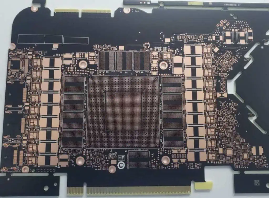
Sectioning by Function
In addition to layers, GPU PCBs organize sections according to function:
The above mockup shows a common breakdown:
- GPU Chip and surrounding power circuitry
- Memory chips / modules and associated power and control logic
- Connectors such as PCIe, display outputs, etc
- Voltage regulator modules (VRMs)
- Specialized support chips like display encoders
This functional division simplifies routing and thermal management.
PCB Production and Refinements
Once designed, PCB production and population involves the following general stages:
1. Fabrication
The board is fabricated by laminating copper layers separated by insulating substrate. Traces are etched, and pads/holes are plated.
2. Component Population
Components are placed and soldered onto the board through techniques like pick-and-place and reflow soldering.
3. Testing and Cutting
The populated boards are electrical and functionally tested. They are then scored and cut into individual PCBs.
4. Coatings and Finishes
Additional coatings and finishes may be applied for protection and aesthetics. Screw holes may also be added.
5. Revisions
Throughout testing, revisions may occur (denoted by Rev 1.0, 1.1 etc) to fix issues prior to mass production.
Role in GPU Performance and Reliability
As illustrated so far, the PCB plays several crucial roles in enabling GPU functionality and performance:
Peak Speeds
Careful trace routing preserves signal integrity for stable peak GPU clock speeds.
Power Handling
Robust power delivery facilitates drawing 100W+ while minimizing ripple for component stability.
Thermal Performance
Heatsinks, pads, heatpipes, and airflow optimizations enable dissipating heavy chip/VRM heatloads.
Environmental Hardiness
Protective coatings and sturdy board materials withstand years of expansion/contraction stress.
In essence, without the interconnects, power delivery, and structural foundation from the PCB, the raw GPU chip and components could not achieve their spectacular speeds and graphics capabilities.
The PCB design thus has an enormous impact on real-world gaming performance and long-term reliability.
PCB Differences Among GPU Tiers
Not all GPUs PCBs share the same design considerations. Lower-cost and higher-mainstream models tend to simplify the PCB to reduce manufacturing costs. This comes at the sacrifice of overclocking headroom and ultimate speed potential.
Meanwhile, premium enthusiast PCBs go all-out, featuring premium materials and significant over-engineering.
Let’s compare various tiers:
Entry-Level GPU PCBs
Found in basic home/office graphics cards. Tend to utilize:
- Basic 2-4 layer PCB
- Simplified power circuitry
- Minimal filtering and protective components
- Reliance on thicker PCB vs additional layers for rigidity
Mainstream GPU PCBs
Features in most gaming GPUs. Offer a balance through:
- 4-8 PCB layers
- Improved power phases and circuit protection
- Some specialized routing for better signal integrity
- Partial coverage of PCB by backplate/shroud for increased rigidity
Enthusiast GPU PCBs
Used on premium GPUs for maximum performance. Identifiable by:
- High layer counts – 8 to 10 typical
- Numerous power phases (14+ common) with high-quality components
- Dual-sided component population
- Elaborate routing for pristine signals
- Copper-reinforced backplate covering much of PCB
- High-end materials (ceramics etc.) for insulation
In general, the more complex and expensive the PCB, the more overclocking headroom and ultimate speed potential from the GPU. Power delivery and heat dissipation also increase markedly across tiers.
Real-World Examples
To illustrate PCB differences, let’s compare boards from entry-level, mainstream, and premium graphics cards:
Entry-Level: AMD Radeon RX 6400
- 4-layer PCB
- Basic 3+1 power phase design
- No backplate
- Partial reinforcement around GPU socket
Mainstream: Nvidia RTX 3060 Ti
- 8-layer PCB
- 7+1 power phases with doublers
- Full backplate with midplate transfer
- Many surface-mounted components
Enthusiast: ASUS RTX 3090 Strix
- 10-layer count
- 19 power phases with premium chokes/MOSFETs
- Full active backplate for cooling VRMs
- Extreme component densities for optimized routing
As you can see, PCBs become markedly more complex and specialized as GPUs scale to premium segments.
These boards enable the high TFLOPs compute, extreme clock speeds, and record-setting benchmark performances endemic to modern flagship GPUs.
Conclusion
In summary:
- The PCB provides the foundation for transforming a raw GPU chip into a fully-functional graphics card.
- Careful board layout facilitates communication between components while managing heat dissipation and electrical needs.
- PCB design directly impacts real-world gaming performance and overclocking potential.
- More premium GPUs utilize specialized PCBs with cutting-edge materials to maximize speeds.
So next time you use a powerful modern video card, take a moment to appreciate the integral role of its underlying printed circuit board!
Frequently Asked Questions
What is the GPU die?
The GPU die or chip is the actual rectangular integrated circuit at the heart of the graphics card. It contains billions of transistors to process graphics and video calculations. The GPU PCB provides the interface to transform this raw chip into a complete product.
What is a VRM?
VRMs (voltage regulator modules) are sets of components that provide stable, clean power to GPU chips and other critical board sections. Quality VRMs ensure smooth power delivery despite heavy, fluctuating power draws.
What is a backplate on a GPU?
A backplate is a protective metal plate mounted onto the backside of the PCB. It prevents board bending, enhances cooling, and provides an aesthetic finish. Backplates are commonly made of aluminum or steel.
Why do more premium PCBs perform better?
Higher-end PCBs use specialized materials and careful layouts with dedicated attention toward signal integrity, heat dissipation, and power delivery. This enables the GPU chip to sustain higher stable clock speeds.
Do graphics cards have other PCBs?
Yes, dedicated graphics cards often have small daughter-boards to host components like video outputs. Larger cards may also use an active backplate PCB to mount supplemental VRMs.