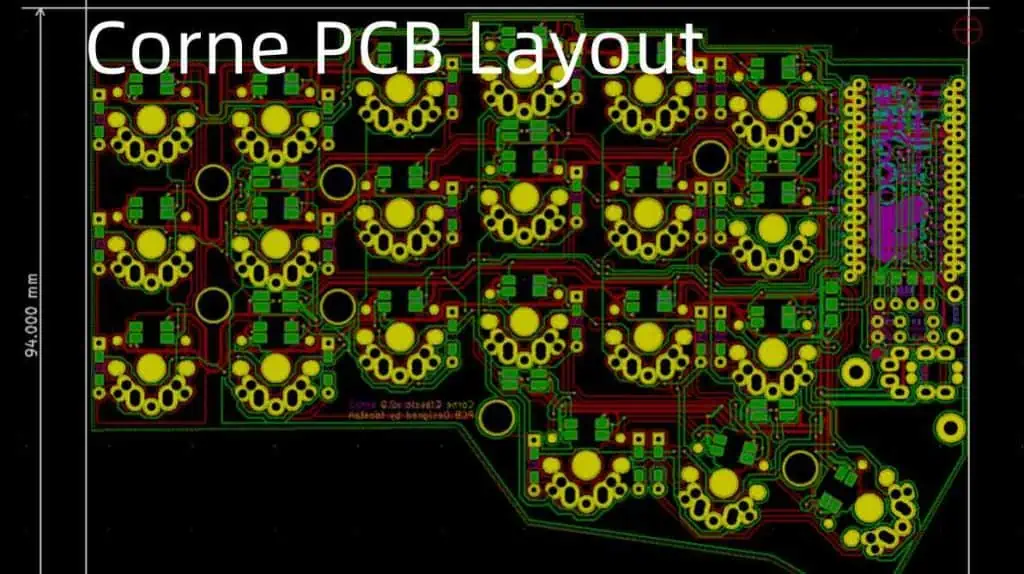
Printed circuit board (PCB) design is an essential engineering function for developing electronic devices and components. PCB designers are highly sought-after to help create circuit boards that are compact, efficient, and robust enough for today’s complex electronics.
Companies seek experienced PCB designers who understand schematics, can effectively use PCB design software, and know how to transform electrical engineers’ functional requirements into optimized board layouts ready for fabrication. Strong communication skills are equally critical for collaborating across engineering teams and manufacturing partners.
This article summarizes commonly asked interview questions for PCB design engineers to assess hard and soft skills relevant to the role. We provide illustrative answers to the questions along with data tables on key PCB design principles that new hires should understand. An FAQ section also covers additional questions candidates have when preparing for PCB design interviews.
Technical PCB Design Interview Questions and Answers

The following are examples of role-relevant technical questions interviewers may ask related to PCB architecture, material selection, component placement, design analysis, and prototyping methods.
1. How do you ensure optimal trace routing in complex multilayer PCBs?
To optimize multilayer PCB trace routing:
- Analyze signal return paths to minimize noise, EMI, and parasitic impedances
- Maintain separation between critical traces to prevent coupling interference
- Balance trace lengths to synchronize timing-critical signals like clocks
- Avoid 90° angles on traces which creates discontinuities that disrupt high-speed signals
- Route clock/data traces orthogonally to isolate signals and minimize crosstalk
- Use wider traces for power to handle required current capacity
- Add shielding (e.g ground planes) between noisy and sensitive circuitry
Proper trace routingminimizes noise, interference, and timing issues in complex PCBs, enabling reliable performance from integrated circuits even at fast clock rates. I would also run signal integrity simulations of proposed PCB stackups using software like HyperLynx to validate trace routing before manufacturing prototypes.
2. How do you manage heat dissipation and thermal issues in PCB design?
To manage PCB thermal issues, I would:
- Identify high-power components early in the design process
- Create local areas on the board to mount heat-sensitive components
- Add thermal vias/pads under hot components to conduct heat into ground planes
- Incorporate exposed copper planes on outer board layers to spread and dissipate heat
- Use PCB finishes like ENIG that enhance thermal transfer
- Simulate airflow across board with CFD software and refine enclosure/cooling approach
- Verify temperature at critical components through thermal imaging of working prototypes
Considering thermal design from the beginning prevents hot spots on circuit boards that can impact device reliability and performance. I collaborate closely with mechanical engineers to optimize cooling system approaches while ensuring the electronics can withstand any vibrations or other environmental conditions.
3. How would you test a new PCB design before manufacturing a full production run?
To fully validate a new PCB design before high-volume manufacturing, I would build and test prototypes in stages:
Stage 1:
- Perform design rule checks and use CAM files for initial prototyping using PCB milling
- Functionally test with breakout boards to check each IC/component
Stage 2:
- Manufacture ~5 test boards from the fabrication house
- Perform bare-board testing to validate electrical connectivity
- Assemble boards to validate functionality against schematics with basic programming
Stage 3:
- Manufacture ~50 pilot run boards
- Test with final assembly (processors, peripherals etc.)
- Run boards for extended soak testing under environmental stress conditions
Prototyping catches design errors early, while pilot runs validate manufacturing and assembly processes. This staged testing lowers risks prior to large-scale PCB fabrication for new products. I work closely with techs and engineers during each test phase and enter issues into bug tracking tools to enable rapid design modifications.
4. How do you ensure manufacturability and DFM (design for manufacturing) in your PCB layouts?
I optimize PCB layouts for manufacturing success and yield by:
- Leaving adequate clearance around pads/vias based on fabrication capabilities
- Adding fiducials for precise alignment during PCB assembly -Using minimum pad sizes for best soldering results and eliminating thermal relief that reduces pad size
- Creating test points to enable quality assurance checking during production
- Selecting standard thicknesses for laminate/copper that match manufacturing inventories
- Defining route paths between pins that allow for chemical etching
- Specifying panel sizes that maximize board quantity per panel production run
I also communicate frequently with our fabrication partners, sending regular design updates and discussing any potential manufacturability issues I foresee in layouts. This design-for-manufacturing (DFM) approach prevents delays and unnecessary costs in Readying designs for volume production.
5. What are some best practices for spacing PCB components and traces?
Some key PCB component and trace spacing best practices include:
- Maintain 2-3x dielectric spacing between traces to prevent short circuits
- Keep 3-5x width spacing between high-speed or noise-sensitive traces
- Allow 5-10x dielectric spacing around integral ICs (e.g. microprocessors)
- Place 0402 size passives 0.1mm apart, while larger components need 0.2mm spacing
- Ensure adequate clearance between traces and edges/holes to account for fabrication tolerance
- Use wider gaps (up to 25x dielectric) for very high voltage traces (>100V)
- Keep soldermask expansion modest (0.075mm) to prevent exposed copper shorting
I reference IPC standards like IPC-2221 and stay in close contact with fabrication/assembly partners regarding spacing requirements for manufacturability and reliability. Component placement software is invaluable for rapidly validating spacing rules.
6. How would you perform signal integrity analysis on a new PCB layout?
My general signal integrity analysis approach is:
- Identify critical timing paths and interfaces (e.g SPI, USB) on schematics along with their characteristic impedances
- Select PCB stackup using impedance calculators to match transmission line properties
- Route traces for those nets with controlled widths/spacings to achieve impedance targets
- Model transmission lines and attached drivers/receivers in SPICE or IBIS
- Simulate signal waveforms with real world effects like cross-talk to identify reflections/ringing
- Re-route traces as needed to correct issues observed in simulations
- Measure eye diagrams and signal quality on working prototypes using oscilloscope and probing
This workflow validates all signals will have intersymbol interference below permitted thresholds despite noise from high-speed routing complexities. I pay special attention to clock distribution networks which are sensitive to reflections. Signal integrity is key for avoiding errors and timing problems in precision circuit boards.
7. What are some suitable PCB substrate/laminate materials for RF circuits designs?
Good PCB substrate materials for RF designs have consistent dielectric properties, low loss tangents, and use high resistivity laminates:
- PTFE composites like Rogers RO4000 series have stable dielectric constants and low loss
- Ceramic filled PTFE boards provide thermal stability for precision RF circuits
- High frequency/speed FR4 improved for RF performance
- Halogen-free laminates like Isola Astra MT77 meet strict environmental requirements
- Glass reinforced hydrocarbons offer high flexural strength for rigid-flex RF constructions
Material selection depends on balancing cost, thermal capabilities, moisture absorption, Z-axis expansion, and dielectric properties across operating bands and temperatures. I collaborate with RF engineers to model proposed stackups in electromagnetic simulators like Keysight ADS to determine if materials provide adequate isolation and controlled impedances.
8. How would you verify manufacturability constraints are met during PCB layout at companies like ours with 6 mil line/space capabilities?
To confirm my PCB layouts meet or exceed the fabrication constraints at our company such as 6 mil line/space, drill sizes and other tolerances, I would:
- Maintain design rules file specified by the manufacturer inside layout software that enforces their design constraints
- Have our CAM team generate gerber files from my board layouts
- Submit gerbers directly to manufacturer for design rule check through their portal to validate no violations
- Work with fabrication partners on DFM reviews early during layout and modify boards based on their feedback
- Procure test coupons with representative line/space traces for quality assurance
- Visually inspect PCBs under microscope once received to check line widths across layers
This comprehensive strategy ensures manufacturability is built into the design from the start and any capability issues get identified prior to running my layouts through production. I also stay current on process improvement roadmaps from partners to maximize exploitation of latest line resolution and via structure capabilities.
9. What advantages does using through hole vias offer compared to other interconnect options in multilayer PCBs?
Using plated through hole (PTH) vias instead of other via structures offers several advantages for multilayer PCB interconnect:
Reliability
- Proven robust connections between layers with complete plating coverage inside holes
- Does not require filling thus avoids voids which improves thermal transfer
Process Compatibility
- Works with nearly all board fabrication processes (subtractive, semi-additive, etc)
- Enables joining dissimilar laminates since holes span all layers
Layout Flexibility
- Can connect any layer at angles not feasible with staggered/skip vias
- Simplifies routing since traces can jog vertically between signal layers
Cost Savings
- Lower drilling costs compared to using multiple blind/buried vias
- Reduce lamination costs when thicker dielectrics not required for other via approaches
For these reasons, many high reliability or cost-optimized PCB designs still leverage PTH vias for optimal connectivity despite continuing advances in blind/buried via fabrication capabilities.
10. How would you design impedance matched traces to interface with a 25 Gbps NRZ serializer IC in a complex PCB stackup?

Here is my approach to routing 25Gbps single-ended traces matched to serializer ICs:
- Obtain target differential impedance from IC datasheet, usually around 100 Ω
- Use Saturn PCB toolkit to calculate widths/spacings in our board stackup to achieve impedance
- Define matched trace design rules (e.g. 6 mil width / 11 mil spacing to layer 2 refernce)
- Ensure traces have >= 50 mil separation from other nets to minimize interference impact
- Model transmission lines in HyperLynx and simulate with IBIS models to verify impedance tolerance across insertion loss peak
- Implement matched length tuning using meandered geometry if simulations show significant impedance deviations
- Focus on symmetrical routing of the differential pair to provide consistent propagation delay
Close collaboration with signal integrity engineers at each step validates simulations match measured results from working prototypes. Impedance control is critical to allow multi-gigabit serializer ICs to perform reliably.
11. How can you prevent field failures related to electromagnetic interference (EMI) in complex PCBs?
To prevent issues from electromagnetic interference in complex circuit boards, I would employ shielding, component placement/routing approaches that reduce unwanted emissions at key harmonics:
- Use a continuous ground plane to provide low impedance return paths
- Place potential noise sources (processors, crystals, inductors etc) distant from sensitive analog inputs
- Enclose radiating ICs in isolated compartments/cages connected to ground planes
- Design cutouts in planes that form filters blocking emission around critical traces
- Specify ferrite beads, bypass capacitors, and other filtering components
- Validate EMI emission spectrum against regulatory limits by testing prototypes in RF chambers
By dedicating sufficient layout real estate for isolation and control of radiated/conducted interference, I can prevent external noise disrupting inner layer signals in densely packed PCBs operating in noisy environments. Proper EMI management is mandatory for devices like medical equipment with life-critical functions.
12. How do you ensure SPICE circuit simulations correlate accurately to measured data from physical PCB prototype builds?
To accurately correlate PCB simulations to measured data, I work methodically through the following areas to build confidence that simulated behavior mimicks real world performance within acceptable tolerances:
Model Accuracy
- Verify component models used match manufacturer spice/IBIS models for each device’s package/pins/parasitics
- Define boards power architecture from schematics and validate rail sequencing/voltage thresholds
Test Correlation
- Ensure proper test conditions set in spice align to physical hardware test setup
- Correlate results from simulations ‘best case‘ ‘worst case‘ and ‘nominal voltage‘ conditions
Parametric Sweeping
- Run monte carlo simulations sweeping values of critical passives, trace impedances etc through realistic tolerance ranges
- Confirm measured data falls within expectation bands of sweep analysis
Design Iterations
- Tweak component values and routing based on correlation findings
- Progressively reduce differences between simulated estimates and measured characteristics
Through careful, iterative verification of simulation settings and assumptions against real hardware, I can reliably use simulations to predict performance issues and hunt down root causes when prototypes exhibit issues not observed in initial desktop analyses.
13. How would you measure timing delays between key signals during prototype bring-up to validate schematic specifications?
My approach to validate PCB signal timing against schematic requirements would be:
- Identify critical paths like clock distribution, chip selects, resets with timing budgets defined
- Probe waveforms using >1 GHz bandwidth oscilloscope with active probes to minimize loading
- Use marker measurements to quantify timing delays between waveform transitions
- Compare measured intervals to datasheet hold/setup times and schematic jitter allocations
- Capture timing violation windows by deliberately altering clock delays
- Adjust components like series terminations to shape waveforms if measurements fall outside of permitted jitter error bands per protocol specifications
I would capture debug data across operating voltage, current consumption and temperature extremes to validate robust timing margins sufficient for unrelenting part variability and environmental stress over lifelong product operation.
14. How does transmission line theory relate to PCB design? Why is managing transmission line effects important?
Transmission line theory describes how electrical signals propagate along conductors in PCBs. Understanding these effects is key for trace routing in high speed designs:
- Traces over ~1/10 wavelength of signal frequencies act as transmission lines
- Signals exhibit reflected noise, ringning if trace impedances mismatched to source/load
- Eye diagrams show intersymbol interference caused by dispersion/reflections
- Terminations like series resistors reduce reflections but add jitter
- Careful impedance control through trace geometry matching and Reference planes manages transmission line effects
If uncontrolled, transmission line behaviors introduce data errors, electromagnetic interference and prevent reliable performance as data rates rise into the Gbps range. Through precise modeling and layout techniques, I can satisfy impedance targets to ensure clean signal transfer between ICs even with today’s fast edge rates.
15. How could 3D printing be used when developing new PCB boards?
3D printing has a few applications that could help accelerate PCB prototyping:
- 3D print plastic board shapes for trial fitting enclosures
- Print custom jig brackets tailored to hold PCBs during assembly
- Create special test clips that easily interface test gear to boards under test
- Rapidly iterate non-conductive standoff shapes that securely mount boards
- Fabricate initial runs of low-temperature co-fired ceramic substrates via print processes before final LTCC production
- Help visualize board layouts through printing 3D models highlighting component placement
While print quality is generally inadequate for conductive metallic traces on production boards, innovators continually extend 3D printing into more electronics fabrication use cases. As resolution, conductive fill materials and printable dielectric polymers improve, the technology promises toaid PCB designers refine mechanical integration even while boards themselves must use conventional subtractive/additive fabrication means for production runs.
General PCB Design Interview Questions
In addition to testing technical competencies, hiring managers often evaluate a candidate’s soft skills and cultural fit during interviews through open-ended questions like these examples:
1. Describe a case where you successfully delivered a complex PCB project with tight timelines. What challenges did you face and how did you overcome roadblocks?
Early in my career at Glorytech, we won a contract supplying motor controller boards for a major electric vehicle program with an extremely aggressive 4-month deadline from project award to delivering prototypes for design verification.
While our team was excited, I voiced concerns in our planning sessions regarding the schedule risk given several new complex features we aimed to implement that stretched our previous PCB capabilities. Rather than dilute our compelling technical proposal, the engineering lead and I rallied the team to brainstorm parallel paths we could pursue and distributed additional upfront simulation/analysis tasks to derisk elements identified on the critical path.
Leveraging lessons learned from prior projects, I optimized component placement for thermal performance and manufacturing efficiency while also