A printed circuit board (PCB) is a board made of insulating material like fiberglass with copper tracks printed on it to connect electronic components. PCBs provide the electrical connections between components in an electronic device like computers, mobile phones, appliances etc.
PCB design involves creating schematics and layouts to represent the circuit connections. PCB symbols are graphical symbols used to represent various electronic components and connections in PCB schematic diagrams and layouts. They help engineers visualize the circuit and wiring connections during the design process.
This article will provide an in-depth explanation of what PCB symbols are, the common symbols used, how to read them and use them in PCB design software.
What are PCB Symbols?
PCB symbols are abstract graphical representations of electronic components and connections used in schematic diagrams and PCB layouts.
They allow electrical engineers to visualize complex circuitry and wiring in a simple graphical manner. The symbols depict the function and connections of components without showing the actual physical appearance.
Some key points about PCB symbols:
- PCB symbols represent components like resistors, capacitors, integrated circuits, transistors, connectors, wires and other parts found on a PCB.
- Symbols utilize shapes like rectangles, circles and triangles to depict different components. Lines between symbols show electrical connectivity.
- Symbols are not drawn to scale – they are conceptual abstract representations.
- Each symbol represents a packaged component with two or more pins or leads to connect it to other parts of the circuit.
- Symbols have unique representations across different PCB design software to avoid confusion between similar looking parts.
- Symbols display the component name, value and other information to identify the specific part.
- Standardized symbols from IEC and IEEE allow for consistency and readability across different schematics and layouts.
Overall, PCB symbols provide a simple way for design engineers to conceptualize complex PCB circuits and layouts. The visual language enables efficient schematic capture and layout routing.
Common PCB Symbols
There are hundreds of standard PCB symbols used to represent various electronic components and connections. Here are some of the most common PCB symbols found in schematic diagrams and layouts:
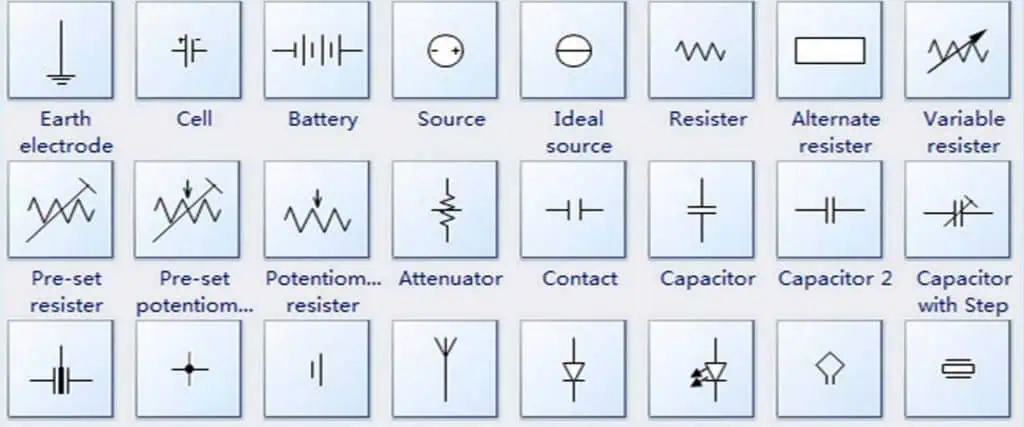
Passive Components
Passive components like resistors, capacitors and inductors have simple but distinct representations:
- Resistor – Zigzag line showing resistance to current flow. Value displayed in ohms (Ω).
- Capacitor – Parallel lines indicating capacitor’s plates to store charge. Value in farads (F).
- Inductor – Coiled wire showing induction of magnetic field. Value in henrys (H).
Active Components
Active components like transistors and integrated circuits (ICs) have more complex symbols:
- NPN Transistor – Arrows show current flow from base to collector. Circle represents base.
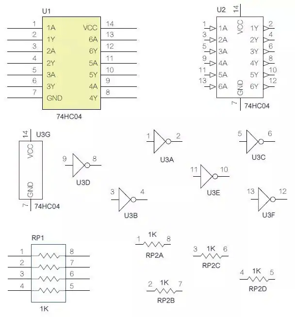
- Integrated Circuit (IC) – Rectangle with pins on sides. Label shows IC name/number.
Connectors
Various connectors are used to interface the PCB with other circuits or devices:
- Male Header – Represented by pin protrusions. Number of pins indicated.
- Female Header – Shows socket holes for male header. Pin count matches male version.
- USB Port – Standard USB symbol used. Indicates host/device with arrow direction.
Power Sources
Power symbols show connections to power sources:
- DC Supply – Indicates DC power source. Positive (+Ve) and negative (-Ve) terminals shown.
- AC Supply – Symbolizes AC power input. May show voltage value.
- Ground – Common ground point for returns.
Miscellaneous
Other common symbols found in PCB schematics and layouts:
- Fuse – Fuse element shown between connections. Current rating displayed.
- Transformer – Two inductive coils coupled by magnetic field.
- LED – Arrow indicates light emission. Longer lead is anode.
- Battery – Voltage rating displayed inside cell symbol.
This covers some of the most prevalent PCB symbols, though there are many more niche representations for specific components and interfaces.
Reading PCB Symbols
Being able to accurately read PCB schematics and layouts requires understanding how to interpret the symbols correctly. Here are some tips on reading PCB symbols:
- Recognize the basic symbol shape – Each component has a distinctive symbol. Learn the common shapes like zigzags, coils, rectangles etc.
- Identify component type from symbol – The symbol directly represents what the component does. For example, capacitor symbols represent a device that stores charge.
- Lookup unfamiliar symbols – Some symbols may be unfamiliar. Refer datasheets or symbol reference charts to identify them.
- Note symbol directions and polarities – Arrowheads indicate current flow direction. Plus/minus signs show polarity.
- Read component names/values – Name and values labeled on symbol provide further identification.
- Follow connecting lines between symbols – Traces between symbols show electrical connectivity in the circuit.
- Match inputs and outputs – Interface points on symbols show connections to other components.
- Note special notations – Symbols may have additional letters, numbers and notes marked.
- Adhere to industry standards – Most symbols follow standards from IEEE and IEC for consistency.
With practice, an engineer proficiently navigates and comprehends PCB schematics and layouts by correctly interpreting all the symbols depicted.
PCB Design Software Symbols
Modern PCB design software provides libraries containing hundreds of standard PCB symbols to use in the tool. Common PCB design software like Altium Designer, Eagle, OrCAD, KiCad etc. include extensive symbol libraries.
Symbols are categorized into components like:
- Passive devices (Resistors, capacitors, inductors etc.)
- Active components (Transistors, ICs, diodes etc.)
- Connectors and interfaces
- Switches, buttons and relays
- Sources (Power supplies)
- Sensors and transducer
- and more
The software libraries provide symbols in all standard orientations – horizontal, vertical, 45° rotated etc. This allows flexibility in positioning symbols in the design diagrams. Engineers can also create custom symbols for specialized components.
PCB software features like Design for Manufacturing (DFM) checks ensure symbols follow accepted industry standards. This aids in proper documentation and production of the board.
PCB Symbol Creation Guidelines
When creating new PCB symbols, engineers should follow these guidelines for clear communication:
- Use distinctive shape for component type
- Include all connection pins/pads
- Mark polarity, pin 1 etc.
- Label part name and values
- Follow industry standards
- Provide symbols in all orientations
- Make symbols clear and easy to recognize
- Test symbols in designs before finalizing
Properly constructed symbols ensure accurate representation of components across the design workflow – from schematics to layout, assembly and testing.
Applications and Use of PCB Symbols
PCB symbols serve important applications throughout the electronics design and manufacturing process:
Schematic Capture – Symbols are used to create circuit schematics showing connectivity between components. Allows system-level visualization.
Simulation – Circuit simulation software leverages component symbols in schematics for functional verification through SPICE models.
PCB Layout – Symbols are mapped to physical footprints on the board during layout.
Bill of Materials – BOM generation tools extract symbols and values from schematics.
Assembly – Component symbols help identify parts for procurement and production.
Servicing – Symbols in schematics allow technicians to diagnose and troubleshoot issues.
Documentation – Symbols provide clear visualization of circuits in documentation like data sheets, manuals, reports etc.
In essence, PCB symbols enable seamless transition of the design through various stages – from concept to final product. Their universal nature makes them vital for standardized communication in the electronics industry.
Symbol Creation Tips
Here are some tips for creating clear and accurate PCB symbols:
–Follow standards – Use existing standards for symbol shapes and conventions. This aids recognition.
–Show connections – Include all relevant pins, terminals, pads etc. to depict electrical nodes.
–Add polarity/direction – Indicate polarity, pin 1 marker and current flow with standard notations.
–Include values – Note resistance, capacitance and other values on the symbol.
–Add labels – Use clear, unambiguous labels for part name, pin names etc.
–Maintain consistency – Use same symbols across schematics, layouts, BOMs etc for clarity.
–Align neatly – Symbols should be aligned properly with neat connecting lines.
–Test systematically – Verify symbol names, values and connections through software checks.
–Get reviews – Have experienced engineers review new symbols to catch any errors.
Proper symbol creation is key for accurate PCB design communication and manufacturing.
Challenges of PCB Symbols

While PCB symbols provide an easy abstraction of complex electronics, some challenges can arise:
- Cluttered schematics – Too many symbols can overcrowd schematics and layouts, making them hard to read.
- Ambiguous representations – Some symbols may not clearly convey the exact component functionality.
- Mismatched libraries – Symbols across tools may not perfectly match, causing confusion.
- Custom symbols – Non-standard custom symbols reduce readability and tool compatibility.
- Updates to standards – Keeping symbol libraries up-to-date with evolving standards is difficult.
- Variation across disciplines – Symbols may vary slightly between electrical, mechanical and software domains.
- Lack of symbol documentation – Symbols without documentation make it hard to interpret their meaning.
Engineers should aim to maximize the benefits of PCB symbols while being mindful of these limitations. Following standards, using consistent libraries and maintaining clean diagrams helps overcome the challenges.
The Future of PCB Symbols
PCB symbol conventions will continue evolving to meet the needs of emerging technologies and design practices:
- New standards – Governing bodies like IEEE/IEC will release updated standards for new components and interfaces. For example, symbols for USB 4.0, DDR5 interfaces etc.
- Smart symbols – Symbols may incorporate more metadata like simulation parameters, lifecycle data etc. for smarter workflows.
- 3D symbols – To complement 3D design workflows, PCB tools could integrate 3D graphical symbols.
- Automated generation – Software solutions to auto-generate symbols from datasheets and 3D models will save effort.
- Multidisciplinary use – Expanding cross-domain use of symbols in electrical, mechanical, software contexts.
- Advanced integration – Seamless usage and conversion of symbols across multiple tools in the design chain.
- Validation checks – Improved automated symbol audits to verify consistency, accuracy and standards conformance.
PCB symbols will adapt to streamline electronics design as technologies continue making exponential advances.
Conclusion
In summary, PCB symbols are the visual language enabling simple and efficient design of complex electronics systems. The concise representations empower rapid schematic creation, hardware-software integration, layout, documentation and manufacturing.
Learning to efficiently leverage PCB symbols is an essential skill for any embedded systems designer and electrical engineer. Their widespread use across the industry underscores their importance at the core of electronics hardware development.
As products advance in complexity and functionality, PCB symbols will continue playing a key role in comprehension and development of sophisticated electronic devices through their simplicity, standardization and universality.
Frequently Asked Questions
Q1: What is the purpose of PCB symbols?
A1: PCB symbols allow engineers to represent components and connections in schematics and layouts visually for simplified design, simulation, production and servicing of electronics hardware. They convey the circuit information efficiently through standardized graphical shapes.
Q2: Should PCB symbols match datasheet symbols?
A2: It is a good practice to match the symbols used in component datasheets to avoid confusion. Many datasheets provide symbols following IEC/IEEE standards that can be reused.
Q3: How are PCB symbols different from schematic symbols?
A3: PCB symbols are a subset of schematic symbols specialized for printed circuit board design. PCB symbols focus on through-hole and SMT components and interconnections on boards.
Q4: Can I use the same PCB symbol in multiple tools?
A4: Yes, you can use PCB symbols across multiple tools like schematic capture, simulation, layout and BOM software. Standard compatible symbols maintain consistency.
Q5: Do symbols change from schematic to PCB layout?
A5: The basic symbol outline usually remains the same. Additional physical details like pad shapes are added in layout. The electrical connections and names stay constant.