Plated through-hole (PTH) vias and standard vias are both conductive holes in a PCB, but they serve different purposes.
A plated through-hole (PTH) is a drilled hole that extends through the entire board and is electroplated with conductive material (typically copper) to form an electrical connection between layers. These holes are often used for component leads (through-hole technology) or as interlayer connections in multilayer PCBs.
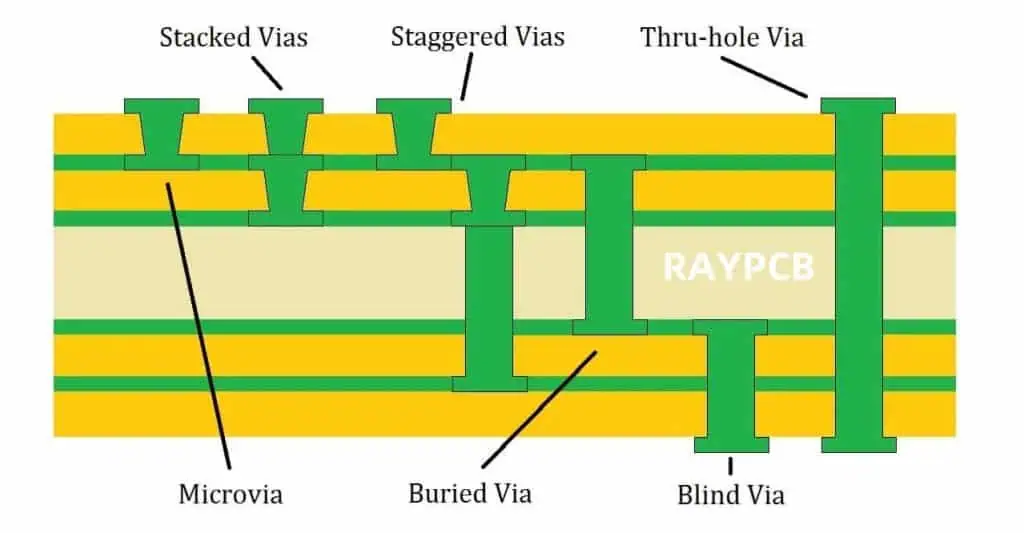
In contrast, a via (blind, buried, or microvia) is a smaller conductive hole that connects specific layers without passing through the entire board. While all PTHs are technically vias, not all vias are PTHs—the key distinction lies in their function and structure.

What are PTH Vias?
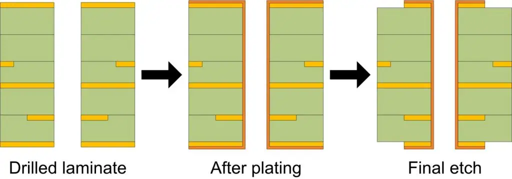
PTH vias, or Plated Through-Hole vias, are conductive pathways that connect different layers of a multilayer printed circuit board. These cylindrical structures are created by drilling holes through the PCB and then plating the inner walls with conductive material, typically copper. PTH vias serve as electrical connections between the various layers of the board, allowing signals and power to flow seamlessly throughout the entire circuit.
Types of PTH Vias
There are several types of PTH vias, each serving a specific purpose in PCB design:
- Through-hole vias: These extend through all layers of the PCB and are used for component leads and interconnections.
- Blind vias: Visible on one side of the board, these connect an outer layer to one or more inner layers.
- Buried vias: These are hidden within the inner layers of the PCB and connect two or more internal layers.
Importance of PTH Vias in PCB Manufacturing
PTH vias play a crucial role in modern electronics, offering several advantages that make them indispensable in PCB manufacturing:
Enhanced Connectivity
PTH vias enable complex routing schemes by allowing signals to pass between multiple layers of a PCB. This capability is essential for creating high-density circuit designs with optimal signal integrity.
Improved Thermal Management
By providing additional pathways for heat dissipation, PTH vias contribute to better thermal management in electronic devices. This is particularly important in high-power applications where heat buildup can lead to performance issues or component failure.
Increased Mechanical Strength
The plated walls of PTH vias add structural integrity to the PCB, reinforcing the connection between layers and improving the overall durability of the board.
Space Optimization
PTH vias allow for more efficient use of PCB real estate by enabling designers to route signals vertically through the board, reducing the need for extensive surface-level routing.
Read more about:
Common Defects in PTH Via Manufacturing
Despite their importance, PTH vias are susceptible to various defects that can compromise the reliability and performance of the PCB. Some common issues include:
Drill Smear
Drill smear occurs when the heat generated during the drilling process causes resin from the PCB material to melt and coat the inner walls of the via. This can prevent proper plating and lead to poor electrical connections.
Voids in Plating
Incomplete or inconsistent plating can result in voids within the via walls. These voids can cause open circuits or intermittent connections, leading to device failure.
Resin Recession
Resin recession happens when the PCB material around the via shrinks during the thermal cycling process, creating a gap between the plating and the board material. This can result in reliability issues and potential device failure.
Copper Wrap Plating Defects
Insufficient copper wrap plating at the top and bottom of the via can lead to weak connections and potential separation of the via from the PCB surface.
Optimizing Drilling Processes for PTH Vias
To improve the yield and reliability of PTH vias, it’s crucial to optimize the drilling process. Here are some key strategies:
Proper Drill Bit Selection
Choosing the right drill bit is essential for creating clean, precise holes. Factors to consider include:
- Drill bit material (e.g., carbide, diamond-coated)
- Drill bit geometry (point angle, flute design)
- Drill bit size and tolerance
Optimizing Drilling Parameters
Fine-tuning drilling parameters can significantly impact the quality of PTH vias:
- Spindle speed
- Feed rate
- Peck drilling techniques
- Entry and exit board materials
Advanced Drilling Technologies
Implementing cutting-edge drilling technologies can enhance via quality:
- Laser drilling for smaller, more precise holes
- Plasma drilling for improved hole wall quality
- Mechanical drilling with advanced control systems
Enhancing Plating Quality and Reliability of PTH Vias
The plating process is critical for ensuring reliable electrical connections in PTH vias. Here are some techniques to improve plating quality:
Desmear and Etchback Processes
Proper desmear and etchback processes remove drilling-induced resin smear and expose the inner layer copper, promoting better adhesion of the plating material.
Optimizing Electroless Copper Deposition
A uniform and adherent electroless copper layer is crucial for subsequent electrolytic copper plating. Factors to consider include:
- Bath chemistry and concentration
- Temperature control
- Agitation methods
Pulse Plating Techniques
Implementing pulse plating can lead to more uniform copper deposition, reducing the risk of voids and improving overall plating quality.
Thermal Stress Management
Addressing thermal stress during the plating process can help prevent issues like resin recession and improve the long-term reliability of PTH vias.
Process Control & Quality Assurance

Maintaining consistent quality in PTH via manufacturing requires robust process control and quality assurance measures:
In-Process Monitoring
Implementing real-time monitoring systems can help detect and address issues during the manufacturing process:
- Drill pressure and spindle speed monitoring
- Plating bath composition analysis
- Automated optical inspection (AOI) for via quality
Statistical Process Control (SPC)
Utilizing SPC techniques can help identify trends and variations in the manufacturing process, allowing for proactive adjustments and improvements.
Non-Destructive Testing Methods
Employing non-destructive testing techniques can provide valuable insights into via quality without damaging the PCB:
- X-ray inspection for internal via structure
- Time-domain reflectometry (TDR) for electrical performance
- Acoustic microscopy for detecting internal defects
Case Studies & Industry Best Practices
Examining real-world examples and industry best practices can provide valuable insights into improving PTH via manufacturing:
Case Study: Automotive Electronics Manufacturer
An automotive electronics manufacturer faced reliability issues with their high-density PCBs due to PTH via failures. By implementing advanced drilling techniques and optimizing their plating process, they achieved a 30% reduction in via-related defects and improved overall product reliability.
Best Practice: Comprehensive Training Programs
Leading PCB manufacturers have found success in implementing comprehensive training programs for operators involved in via drilling and plating processes. These programs focus on understanding the critical parameters and potential defects, empowering operators to make informed decisions and adjustments during production.
Industry Trend: Collaboration with Material Suppliers
Close collaboration between PCB manufacturers and material suppliers has led to the development of advanced laminate materials specifically designed to improve PTH via reliability. These materials offer better thermal stability and reduced z-axis expansion, addressing common issues like resin recession.
Future Trends & Innovations in PTH Via Manufacturing
The field of PTH via manufacturing continues to evolve, with several promising trends and innovations on the horizon:
Additive Manufacturing Techniques
Emerging additive manufacturing processes, such as 3D-printed electronics, may revolutionize the way PTH vias are created, offering greater design flexibility and potentially reducing manufacturing costs.
Advanced Materials
Development of new PCB materials with improved thermal and electrical properties may address some of the current challenges in PTH via reliability, particularly in high-frequency and high-power applications.
Artificial Intelligence in Process Control
The integration of AI and machine learning algorithms into process control systems could lead to more adaptive and efficient manufacturing processes, optimizing via quality in real-time based on complex data analysis.
Miniaturization and High-Aspect-Ratio Vias
As electronic devices continue to shrink, the demand for smaller, higher aspect ratio PTH vias is increasing. This trend is driving innovations in drilling and plating technologies to achieve reliable connections in increasingly compact designs.
In conclusion, PTH vias remain a critical component in PCB manufacturing, playing a vital role in the functionality and reliability of electronic devices. By focusing on optimizing drilling and plating processes, implementing robust quality control measures, and staying abreast of emerging trends and technologies, manufacturers can significantly improve the yield and reliability of PTH vias. As the electronics industry continues to evolve, the importance of high-quality PTH vias will only grow, making ongoing research and innovation in this field essential for meeting the demands of future electronic designs.