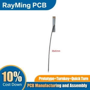
Proper PCB antenna placement is crucial for optimal performance. Place antennas away from metal components and high-frequency signals to avoid interference. Ensure a clear ground plane and maintain sufficient distance from other circuitry. Use impedance matching and consider antenna orientation for better signal reception. Test and optimize placement during prototyping for best results.

Don’t lose 90% of total efficiency by poorly placing your PCB antenna!
Main points:
1) Optimal ground plane size is 1/4lambda
2) Keep-out area – no metal around antenna
3) No big metal components near antenna
The strategic placement of antennas on printed circuit boards (PCBs) represents one of the most critical aspects of wireless device design. Poor antenna placement can severely compromise signal quality, reduce transmission range, and create interference issues that plague device performance. Understanding the fundamental principles and practical techniques for optimal antenna positioning is essential for engineers developing everything from IoT sensors to high-performance communication devices.
Understanding Antenna Fundamentals in PCB Design
Antennas function by converting electrical energy into electromagnetic waves and vice versa. On a PCB, this conversion process is heavily influenced by the surrounding environment, including ground planes, traces, components, and even the device enclosure. The antenna’s radiation pattern, gain characteristics, and impedance matching all depend critically on its physical placement and the electromagnetic environment created by the PCB layout.
The most fundamental consideration in antenna placement is maintaining a clear radiation pattern. Antennas require unobstructed space to radiate efficiently, and any nearby conductive elements can significantly alter their performance characteristics. This includes not only obvious obstructions like large metal components but also subtle influences from ground planes, power traces, and even small passive components positioned too closely to the antenna element.
Ground Plane Considerations and Keep-Out Zones
Ground planes play a pivotal role in antenna performance, serving as both a reference for the antenna and a potential source of interference. The relationship between the antenna and ground plane must be carefully managed to optimize performance. For most antenna types, maintaining appropriate clearance from ground planes is crucial for preserving the intended radiation pattern and preventing detuning effects.
Establishing proper keep-out zones around antennas is essential for consistent performance. These zones should be free from copper pours, traces, vias, and components that could interfere with the antenna’s electromagnetic field. The size of these keep-out zones varies depending on the antenna type and operating frequency, but generally extends at least one-quarter wavelength from the antenna element in all directions where possible.
The ground plane size and shape also significantly impact antenna performance. For chip antennas and PCB trace antennas, the ground plane acts as a counterpoise, and its dimensions directly affect the antenna’s resonant frequency and radiation efficiency. Insufficient ground plane area can lead to poor antenna efficiency and unpredictable performance variations across different device orientations.
Minimizing Interference from Digital Circuits
Modern PCBs typically combine wireless functionality with digital processing circuits, creating potential interference challenges. Digital switching circuits generate broadband electromagnetic noise that can couple into antenna systems, degrading receiver sensitivity and creating spurious emissions. Careful placement strategies can minimize these interactions and maintain clean RF performance.
Physical separation represents the first line of defense against digital interference. Positioning antennas as far as possible from high-speed digital circuits, crystal oscillators, and switching power supplies helps reduce coupling mechanisms. When physical separation is limited by board size constraints, strategic use of ground planes and shielding techniques becomes critical.
Clock signals and their harmonics pose particular challenges for antenna systems. High-frequency clock edges create broadband noise that can interfere with receiver circuits across multiple frequency bands. Routing clock signals away from antenna areas and using proper grounding techniques helps minimize these effects. Additionally, implementing spread-spectrum clocking can reduce the peak energy at specific frequencies, making interference management more manageable.
Multi-Antenna Systems and Diversity Techniques
Many modern wireless devices incorporate multiple antennas to improve performance through diversity techniques or multiple-input multiple-output (MIMO) systems. The placement of multiple antennas on a single PCB requires careful consideration of mutual coupling effects and correlation between antenna elements.
Antenna spacing plays a crucial role in diversity system performance. For spatial diversity applications, antennas should be separated by at least half a wavelength to ensure sufficient decorrelation between received signals. However, physical constraints often limit achievable spacing, making pattern diversity and polarization diversity attractive alternatives.
Pattern diversity can be achieved by orienting antennas in different directions or using different antenna types with complementary radiation patterns. This approach allows for effective diversity performance even when physical spacing is limited. Polarization diversity employs antennas with orthogonal polarizations, such as combining vertical and horizontal linear polarizations or using circular polarizations of opposite handedness.
Frequency-Specific Placement Strategies
Different frequency bands present unique challenges and opportunities for antenna placement. Low-frequency applications, such as those operating in the 433 MHz or 915 MHz ISM bands, typically require larger antenna structures and more extensive keep-out zones. The longer wavelengths associated with these frequencies make quarter-wave and half-wave antenna elements physically large, often requiring creative placement solutions or the use of loading techniques to reduce antenna size.
Higher frequency applications, including 2.4 GHz Wi-Fi, Bluetooth, and 5 GHz systems, benefit from smaller antenna structures but face increased sensitivity to nearby objects and manufacturing tolerances. The shorter wavelengths make these systems more susceptible to detuning effects from nearby components and mechanical variations in the manufacturing process.
Millimeter-wave applications, such as those used in 5G communications and high-resolution radar systems, present extreme challenges for PCB antenna placement. The very short wavelengths make these systems highly sensitive to even minor placement variations, requiring precise design practices and careful attention to manufacturing tolerances.
PCB Stack-Up Considerations
The PCB stack-up significantly influences antenna performance, particularly for antennas implemented directly on the PCB using copper traces. The dielectric constant and loss tangent of the PCB substrate material affect the antenna’s resonant frequency, bandwidth, and efficiency. These effects must be considered during the design phase and may require antenna geometry adjustments to compensate for the substrate properties.
Multi-layer PCB designs offer opportunities for improved antenna integration through the use of dedicated antenna layers and optimized ground plane configurations. However, the increased complexity of multi-layer designs also introduces additional variables that can affect antenna performance, including layer-to-layer registration tolerances and via placement effects.
Mechanical and Thermal Considerations
Antenna placement must account for mechanical stress and thermal effects that can occur during device operation and environmental exposure. Antennas positioned near mechanical stress points or areas subject to significant temperature variations may experience performance degradation over time. This is particularly important for devices intended for automotive, industrial, or outdoor applications where environmental conditions can be severe.
Thermal management becomes critical when antennas are placed near power-dissipating components. Elevated temperatures can affect the electrical properties of antenna materials and nearby dielectric substrates, potentially causing frequency shifts and performance degradation. Proper thermal design practices, including the use of thermal vias and heat spreaders, help maintain stable antenna performance across the intended operating temperature range.
Testing and Validation Strategies
Successful antenna placement requires comprehensive testing and validation to ensure performance meets design requirements across all intended operating conditions. This includes both simulation-based analysis during the design phase and physical measurements of prototype hardware. Antenna measurement techniques must account for the complete system environment, including the effects of nearby components, enclosures, and user interaction.
Over-the-air testing in realistic environments provides the most accurate assessment of antenna system performance. This includes evaluation of radiation patterns, gain characteristics, and interference susceptibility under conditions that closely match the intended application. Such testing often reveals performance issues that are not apparent in idealized simulation environments or laboratory measurements.
Conclusion
Effective PCB antenna placement requires a comprehensive understanding of electromagnetic principles, careful attention to design details, and systematic validation through simulation and measurement. The techniques and considerations outlined here provide a foundation for achieving optimal antenna performance in modern wireless devices. Success in antenna placement comes from balancing competing requirements while maintaining focus on the specific performance metrics most critical to the intended application. As wireless technologies continue to evolve and integrate into increasingly compact devices, these fundamental principles remain essential for achieving reliable and efficient wireless communication systems.