Introduction
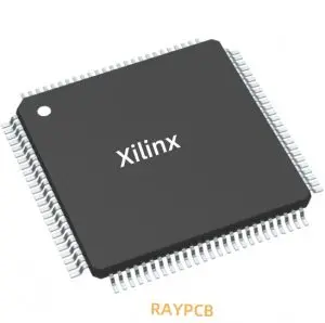
The XQ2V1000 is a defense-grade Field-Programmable Gate Array (FPGA) from Xilinx’s QPro Virtex-II Military QML Platform FPGA family. Designed specifically for high-reliability aerospace and defense applications, the XQ2V1000 offers 1 million system gates and combines robust performance with military-grade reliability. This device leverages advanced 0.15μm/0.12μm CMOS 8-layer metal process technology to deliver high-speed operation with optimized power consumption for mission-critical systems.
Device Overview
The XQ2V1000 sits within Xilinx’s QPro Virtex-II platform FPGA family, which was introduced in January 2001 and represented a significant advancement in FPGA technology for military and aerospace applications. With its 1 million system gate capacity, the XQ2V1000 provides a powerful and flexible platform for implementing complex digital systems in harsh environments. The “XQ” prefix designates its military qualification, while the “2V1000” indicates its position in the Virtex-II family with approximately 1 million system gates.
Powered By EmbedPress
Key Features
Logic Resources
- System Gates: 1 million system gates
- Configurable Logic Blocks (CLBs): Arranged in rows and columns
- Slices: Each CLB contains two slices, with each slice containing two function generators
- Look-Up Tables: Four-input LUTs for implementing any four-input Boolean function
- Flip-Flops: Storage elements for sequential logic
- Block RAM: Dual-port 18Kb blocks with configurable width and depth
- Distributed RAM: Flexible memory implementation using CLB resources
Processing Capabilities
- Clock Management: Digital Clock Manager (DCM) for clock distribution and phase control
- Multiplier Blocks: Dedicated 18×18 hardware multipliers
- Maximum Frequency: Up to 650 MHz (speed grade dependent)
- Fast Carry Logic: For arithmetic operations and counters
Connectivity
- I/O Standards: Support for numerous single-ended and differential I/O standards
- I/O Banking: Multiple independently configurable I/O banks
- LVDS Support: High-speed differential signaling capability
- DDR Support: Double Data Rate interface capability
- PCI Compatible: Support for 33 MHz PCI interface
Special Features
- Military Qualification: Certified to MIL-PRF-38535 (Qualified Manufacturer Listing)
- Temperature Range: Full military temperature range (-55°C to +125°C)
- Enhanced Reliability: 100% factory tested for mission-critical applications
- Configuration: Multiple configuration options including JTAG, SelectMAP, and Serial mode
- IP-Immersion Architecture: Support for IP core-based design implementation
Military-Grade Specifications
The XQ2V1000 offers enhanced reliability through:
- MIL-PRF-38535 qualification
- Full military temperature range operation (-55°C to +125°C)
- 100% factory testing
- Available in Q-grade (quality) specification
- Enhanced reliability screening
Power Specifications
- Core Voltage: 1.5V core operation
- I/O Voltage: Configurable per bank
- Power Management: Multiple power-saving features
Package Options
The XQ2V1000 is available in several package options:
- BG575: 575-pin Ball Grid Array package
- FF896: 896-pin Fine-pitch BGA package
- FG456: 456-pin Fine-pitch BGA package
- Ceramic and Plastic Options: For varied application requirements
Applications
The XQ2V1000 is particularly suited for mission-critical applications including:
- Military communications systems
- Aerospace control systems
- Radar and sonar processing
- Electronic warfare systems
- Satellite systems
- Mission-critical data processing
- Secure communications
- Avionics
- Missiles and munitions guidance
Architecture Details
Configurable Logic Blocks (CLBs)
The XQ2V1000 features a coarse-grained architecture consisting of Configurable Logic Blocks (CLBs) arranged in rows and columns. Each CLB consists of four logic cells arranged in two slices. Each slice contains:
- Two function generators (implemented as 4-input LUTs)
- Two storage elements (flip-flops)
- Arithmetic logic gates
- Multiplexers
- Fast carry look-ahead chain
- Horizontal cascade capability
Memory Resources
Memory in the XQ2V1000 is implemented through a hierarchy of resources:
- Block SelectRAM: 2.5Mb of dual-port RAM in 18Kb blocks
- Distributed SelectRAM: Up to 1Mb of memory implemented in CLBs
- Flexible memory configuration options for width and depth
Clock Management
The XQ2V1000 includes Digital Clock Manager (DCM) blocks that provide:
- Clock distribution with minimal skew
- Frequency synthesis
- Phase shifting
- Domain crossing capabilities
Input/Output Features
The device offers versatile I/O capabilities:
- Multiple I/O banks with independent voltage standards
- Support for numerous single-ended standards (LVTTL, LVCMOS, etc.)
- Support for differential standards (LVDS, HSTL, etc.)
- Dedicated DDR support for high-bandwidth memory interfaces
- PCI compliance for system integration
Development Tools Support
The XQ2V1000 is supported by:
- Xilinx ISE Design Suite for design implementation
- ModelSim for simulation
- ChipScope for on-chip debugging
- System Generator for DSP for algorithm implementation
- IP cores for accelerated design implementation
Ordering Information
When ordering the XQ2V1000 device, the complete part number follows this format: XQ2V1000-[Speed Grade][Package][Temperature Grade]
Example: XQ2V1000-4BG575N
- XQ2V1000: Device name
- 4: Speed grade (-4, -5, or -6 available)
- BG575: 575-pin Ball Grid Array package
- N: Industrial temperature grade (or M for military)
Conclusion
The XQ2V1000 provides a robust platform for implementing complex digital systems in demanding military and aerospace applications. With its million-gate capacity, versatile I/O capabilities, and military qualification, this defense-grade FPGA delivers reliable performance for mission-critical systems. As part of Xilinx’s QPro Virtex-II family, the XQ2V1000 represents a mature technology with established reliability and well-documented design methodologies, making it suitable for long-lifecycle defense and aerospace programs where reliability is paramount.
For complete specifications and detailed information, please refer to the official Xilinx (now AMD) documentation including the QPro Virtex-II Military QML Platform FPGAs Datasheet and the Virtex-II Platform FPGA User Guide.

