Mounting Type: Surface Mount
Logical Description: IC, Xilinx DS170 XA Spartan-6 Automotive FPGA Family
Physical Description: Ball Grid Array (BGA), 0.80 mm pitch, square; 225 pin, 13.00 mm L X 13.00 mm W X 1.40 mm H body
Product Attributes
| Maximum Number of User I/Os : 160 | Number of Registers: 18224 |
| RAM Bits: 576Kbit | Device Logic Cells: 14579 |
| Process Technology: 45nm | Number of Multipliers: 32 (18×18) |
| Programmability: Yes | Program Memory Type: SRAM |
| Minimum Operating Temperature: -40°C | Maximum Operating Temperature: 125°C |
| Dedicated DSP: 32 | Speed Grade: 2 |
| Device Number of DLLs/PLLs: 6 | Total Number of Block RAM: 32 |
| Basic Package Type: Ball Grid Array | Package Family Name: BGA |
| Package Description: Chip Scale Ball Grid Array | Lead Shape: Ball |
| Pin Count: 225 | PCB: 225 |
| Mount: Surface Mount | MSL: 3 |
| Maximum Reflow Temperature (°C): 260 | Reflow Solder Time (Sec): 30 |
| Number of Reflow Cycle: 3 |
For Use With

Overview
The Xilinx XA Spartan-6 Automotive FPGA family delivers low-cost, reliability-optimized programmable logic for automotive applications. Within this family, the XA6SLX16-2CSG225Q provides a balance of logic density, features, and thermal performance.
In this article, we will take a look at the key capabilities and specifications of the XA6SLX16 from its datasheet and reference manual. We’ll examine its programmable logic, embedded blocks, I/O, package, reliability, and other details relevant to automotive usage.
XA6SLX16 FPGA Characteristics
The XA6SLX16 sits in the middle of the Spartan-6 XA family with these high-level characteristics:
Programmable Logic
- 16,000 logic cells
- 1008 Kb (504×2) block RAM
- 12 DSP slices
I/O
- 225 general purpose I/O pins
- Support for common standards (LVDS, LVPECL, SSTL)
Clock Management
- 7 clock management tiles with DCM and PLL
- Sub-ns clock skew matching
Configuration
- SPI and BPI flash loading
- MultiBoot support for safe firmware updates
Packages
- 225-pin BGA package
- 15mm x 15mm, 0.8mm pitch
- Supported temperature -40C to +125C
This provides a solid amount of logic, I/O, and routing in a relatively compact footprint.
FPGA Logic Cells
The core programmable logic inside the XA6SLX16 consists of 16,000 logic cells arranged in a matrix of CLBs (configurable logic blocks):
- Each CLB contains 4 slices, each with 4 6-input LUTs and 8 flip-flops
- 160 D-type flip-flops per CLB for register-heavy designs
- Arithmetic carry chains for high performance math
In addition to basic logic, the FPGA contains dedicated routing for high-speed connections:
- Direct connections between adjacent CLBs
- Low-skew global clock networks
- Fast carry chains for arithmetic
- Low-latency bypass paths
These optimize performance for real-time automotive systems.
Block RAM
For data buffering and memory storage, the XA6SLX16 contains 1008 Kb of fast block RAM in 504 dual-port 18 Kb blocks.
Key capabilities:
- True dual port for simultaneous access
- Configurable as single 36 Kb RAM
- Byte write enable for partial updates
- Optional ECC for safety-critical data
- 6500 memory access per second
The ample block RAM enables data processing without external memories.
DSP Slices
For digital signal processing, the FPGA includes 12 dedicated DSP slices. Each slice provides:
- 25×18 bit signed multiply with 48-bit accumulate
- Fast parallel multiply accumulation
- Pipelining and shifting capabilities
- Cascadable to 72-bits for high precision
DSP use cases include filters, FFTs, digital modulation, and more.
Clock Management
The XA6SLX16 contains 7 clock management tiles (CMTs), each including a mixed-mode clock manager (MMCM) and digital clock manager (DCM).
Key features:
- Clock synthesis from 6-740 MHz
- Zero delay buffers, low skew routing
- Phase aligned clocking for high speed data
- Input jitter filtering
- Precision clock division and multiplication
This enables low noise system clocks derived from common automotive oscillator sources.
I/O Capabilities
With 225 I/O pins, the XA6SLX16 can interface to a wide range of automotive peripherals and signals.
I/O Support:
- 1.2V to 3.3V signaling
- LVDS, LVPECL, differential inputs
- SSTL, HSTL, LVCMOS standards
- SDR and DDR interfacing up to 800Mbps
- High current drive up to 24mA
- Slew rate and impedance control
Banks of I/O pins are grouped into power domains that can be shut off when unused. This allows optimizing I/O power consumption.
Configuration and Security
The XA Spartan-6 supports both SPI and parallel BPI flash for configuration:
- MultiBoot enables safe dual-image firmware updates
- AES-GCM 256-bit encryption secures bitstream
- RSA authentication prevents tampering
- Battery-backed RAM for key storage
Robust protections against tampering assist functional safety certifications.
Automotive Reliability
The XA family undergoes additional qualification for automotive environments:
- AEC-Q100 Grade 2 qualified production flow
- Full Xilinx standard qualification flow
- Production monitory and change control
- Zero defects and fit policy
- Extended -40C to +125C temperature range
- MTTF >100 years for safety-critical applications
This level of qualification provides confidence for deploying XA FPGAs in vehicle systems.
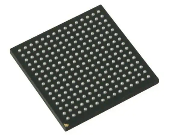
XA6SLX16 Packaging
The 225-pin 15mm x 15mm ball grid array package offers flexibility in PCB mounting:
FPGA Ball Map:
Relevant specifications:
- 1mm ball pitch for routing access
- Lead-free solder process
- Corner chamfer indicates pin 1 location
- Solid BGA balls for improved thermal conduction
The compact footprint fits space constrained PCBs while allowing sufficient routing escape. A thermal pad improves heat dissipation to the PCB.
Development Tools
Xilinx provides multiple options for developing with the XA6SLX16, including:
- Xilinx ISE Design Suite for RTL synthesis and Place and Route
- SDAccel development environment for OpenCL designs
- SoftConsole integrated development environment (IDE)
- Hardware debugging using ChipScope Pro and SignalTap analysis
These represent a mature, full-featured toolchain for developing and deploying XA6SLX16 designs.
Conclusion
With its automotive-grade qualification, security features, logic density, and blend of programmable logic and hardened blocks, the Xilinx XA6SLX16-2CSG225Q FPGA provides a compelling option for automotive applications like ADAS, infotainment, and digital instrument clusters. Engineers can take advantage of its optimized price/performance/power for embedded vision, sensor interfacing, and real-time control systems in next-generation vehicles.
Frequently Asked Questions
Q: What are the main advantages of the XA Spartan-6 family compared to a microcontroller?
A: FPGAs provide custom hardware parallelism, real-time responsiveness, and hardware-based reliability compared to sequential microcontroller execution.
Q: What is the difference between the XA Spartan-6 vs standard Spartan-6 FPGAs?
A: The XA family has additional automotive qualification, extended temperature range, multi-time programming fuse, AES encryption, and other features tailored for automotive.
Q: How is configuration firmware loaded onto the XA6SLX16 FPGA?
A: An external SPI or parallel flash is used to load the bitstream at power up. MultiBoot provides dual-image support.
Q: What is the typical static (leakage) power consumption of the XA6SLX16?
A: Depending on configuration, 20-100 mW is typical. Power gating domains and shutdown allow minimizing static power.
Q: What tools are available for developing with the XA6SLX16 FPGA?
A: Xilinx provides the ISE, Vivado, and SDAccel toolchains. SoftConsole is available as an IDE. Simulation, place and route, and debugging tools are included.