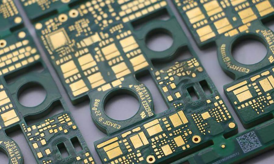
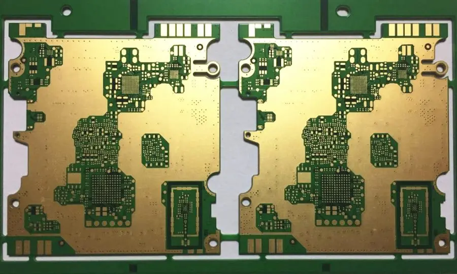
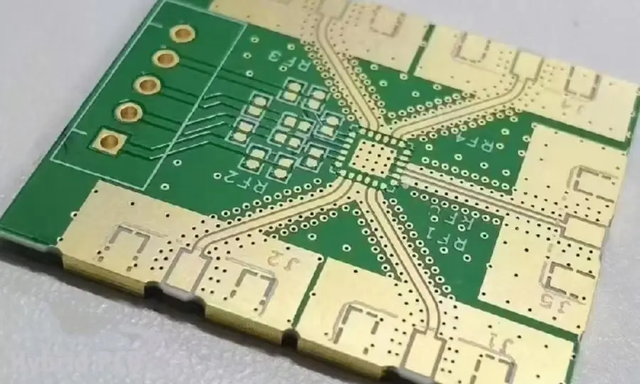
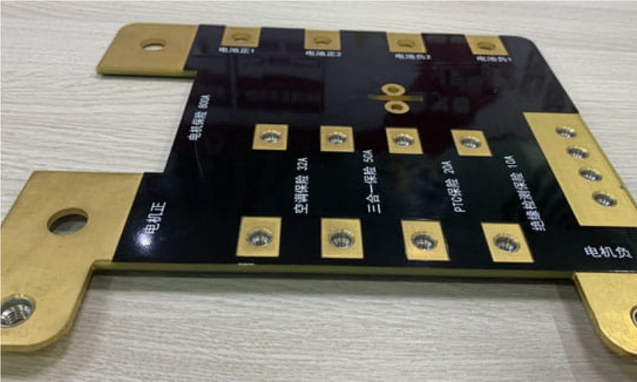
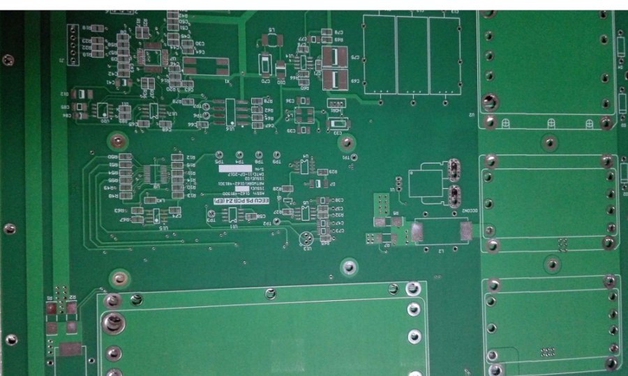
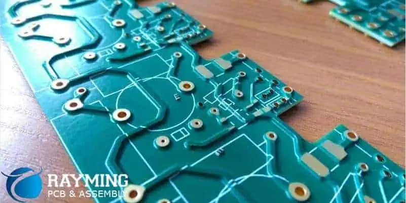
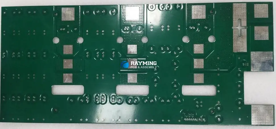
Rayming specializes in heavy copper PCB manufacturing, supporting copper weights up to 20 oz. Our experienced team excels in solder mask printing and maintains stringent quality controls to ensure superior performance in extreme copper PCB applications.
A heavy copper PCB is a specialized printed circuit board featuring copper layers significantly thicker than standard PCBs. While conventional PCBs typically use copper weights ranging from 0.5 oz to 3 oz per square foot (17.5μm to 105μm), heavy copper PCBs are characterized by copper thicknesses of 3 oz/ft² or greater, with some applications requiring up to 20 oz/ft² (700μm) or even extreme copper weights reaching 200 oz/ft².
| PCB Type | Copper Weight | Thickness | Typical Applications |
|---|---|---|---|
| Standard PCB | 0.5-3 oz/ft² | 17.5-105μm | Consumer electronics, basic circuits |
| Heavy Copper PCB | 3-20 oz/ft² | 105-700μm | Power electronics, automotive, industrial |
| Extreme Copper PCB | 20-200 oz/ft² | 700-7000μm | High-power military, aerospace systems |
The copper weight measurement represents the weight of copper that would cover one square foot of the PCB surface, making it a standard industry metric for specifying copper thickness across different PCB types.
Understanding the fundamental differences between heavy copper and standard PCBs is crucial for making informed design decisions.
The most significant advantage of heavy copper PCBs lies in their superior current-carrying capacity:
Current Calculation Example: For a 5mm wide trace with a 20°C temperature rise:
Heavy copper PCBs excel in thermal management due to copper’s exceptional thermal conductivity (401 W/m·K):
The increased copper thickness provides enhanced mechanical properties:
Heavy Copper PCB Calculator
RayPCB Engineering Tools
🔄 Copper Weight Converter
📊 Standard Copper Weights Reference
| Weight | mm | mils | µm | Type |
|---|---|---|---|---|
| 0.5 oz | 0.0175 | 0.69 | 17.5 | Standard |
| 1 oz | 0.035 | 1.38 | 35 | Standard |
| 2 oz | 0.070 | 2.76 | 70 | Standard |
| 3 oz | 0.105 | 4.13 | 105 | Heavy |
| 4 oz | 0.140 | 5.51 | 140 | Heavy |
| 6 oz | 0.210 | 8.27 | 210 | Heavy |
| 10 oz | 0.350 | 13.78 | 350 | Extreme |
| 20 oz | 0.700 | 27.56 | 700 | Extreme |
⚡ Current Carrying Capacity (IPC-2221)
📈 Current Capacity Comparison
For 100 mil trace width @ 20°C rise (External)
📐 Trace Width Calculator
🔍 Visual Trace Comparison
Trace width needed for 15A @ 20°C rise
🌡️ Thermal Resistance Calculator
📋 Thermal Properties Comparison
PCB Layer Stack Visualization
Heavy copper increases thermal mass and heat spreading capability
💰 Heavy Copper PCB Cost Estimator
📊 Cost Factors Breakdown
Relative cost impact of heavy copper vs standard PCB
Click on each tip to expand detailed design guidelines for heavy copper PCBs.
Minimum Trace Width: Heavy copper requires wider minimum traces due to etching undercut. For 3oz copper, minimum trace is typically 8-10 mils; for 6oz, it's 12-15 mils; for 10oz+, expect 20+ mils minimum.
Spacing Rules: Increase spacing proportionally with copper weight. Use 1:1 ratio as a starting point (trace width = spacing). For high voltage, increase spacing per IPC-2221 guidelines.
Tip: Design with 20% margin above minimums to improve yield and reduce cost.
Via Size: Use larger vias for heavy copper (minimum 0.4mm drill for 3oz, 0.5mm for 6oz+). The aspect ratio (board thickness/hole diameter) should not exceed 8:1.
Via Arrays: For high current, use multiple vias in parallel. Calculate total current capacity as sum of individual via capacities minus 20% for thermal coupling.
Thermal Vias: Place thermal vias directly under heat-generating components with 0.3-0.5mm pitch. Fill with solder or conductive epoxy for best thermal transfer.
Symmetrical Design: Always use symmetrical copper distribution to prevent board warping. If outer layers are 4oz, balance with inner power/ground planes.
Prepreg Selection: Use high-resin content prepreg (≥60%) to fill the gaps caused by thick copper features. Multiple prepreg sheets may be needed.
Mixed Copper: Consider using heavy copper only where needed (power paths) and standard copper for signal layers to optimize cost and manufacturability.
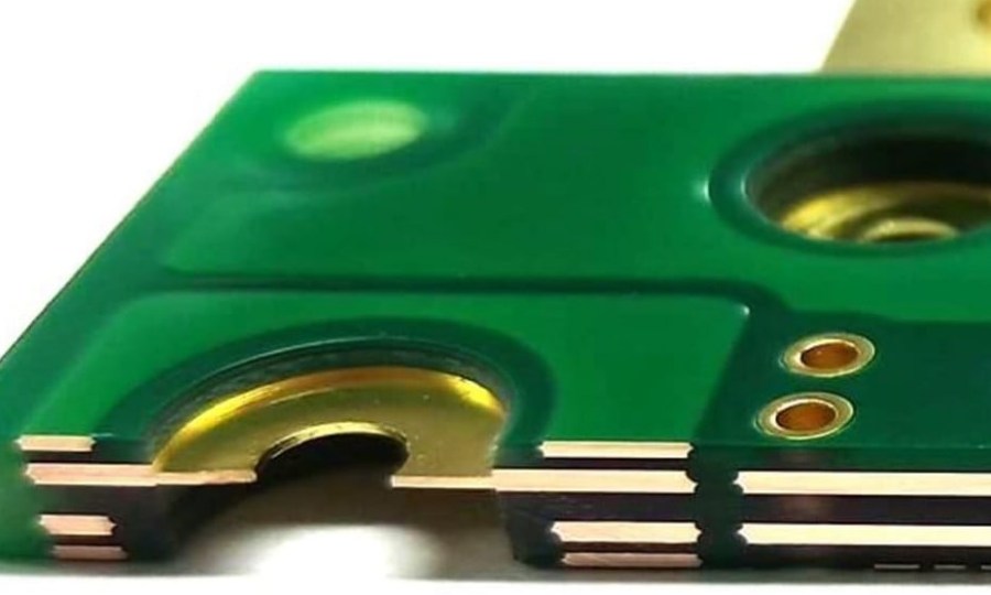
Coverage Challenges: Heavy copper creates significant height differences. Standard solder mask may not adequately cover trace edges, leading to exposed copper.
Solutions: Request multiple solder mask coats, use liquid photoimageable (LPI) solder mask, or consider selective solder mask with exposed copper planes for better thermal performance.
Design Rule: Increase solder mask clearance by 2-3 mils per ounce of copper above 2oz to account for registration challenges.
Copper Planes: Maximize copper pour areas for heat spreading. Use polygon pours connected to power components. Avoid isolated copper islands that can't dissipate heat.
Component Placement: Distribute heat sources evenly. Keep high-power components away from board edges where heat can't spread in all directions.
Airflow: Orient traces parallel to expected airflow direction. Place thermal relief patterns on pads connected to large copper areas for reliable soldering.
Undercut Effect: Thick copper etches more at the base than the top, creating trapezoidal trace profiles. Plan for ~1mil undercut per ounce of copper on each side.
Compensation: Work with your fab to determine etch compensation factors. Typically add 0.5-1.0 mils per ounce to designed trace widths.
Isolation: Large copper areas may need isolation slots or breakup patterns to ensure complete etching and prevent shorts from bridged copper.
Panelization: Heavy copper boards need larger panel margins and breakaway tabs due to increased mechanical stress during depaneling.
Tooling Holes: Use larger tooling holes (≥3.2mm) with adequate clearance from copper features to prevent damage during handling.
Documentation: Clearly specify copper weights for each layer in fab notes. Include cross-section drawings for complex stackups. Communicate current requirements to help fab optimize the design.
Electrical Testing: Request 100% electrical testing for heavy copper boards due to higher risk of shorts from etching challenges.
Cross-Section Analysis: For critical applications, request cross-section samples to verify copper thickness, via plating quality, and layer registration.
Thermal Cycling: Heavy copper PCBs may experience different thermal expansion. Consider thermal cycling tests for high-reliability applications to verify long-term solder joint integrity.
🏭 RAYPCB Heavy Copper Capabilities
📦 Applications & Lead Times
Typical Applications
Estimated Lead Times
Heavy copper PCBs can handle continuous high-current loads without the voltage drops and heating issues common in standard PCBs. This capability is essential for:
The thick copper layers act as integrated heat spreaders, eliminating the need for external thermal management solutions in many applications:
Heavy copper technology enables more compact designs by:
For high-frequency applications, heavy copper provides:
While initial PCB costs are higher, heavy copper boards offer long-term savings through:
Heavy copper PCBs are fundamental to modern power electronics:
Power Supplies and Converters
Motor Drives and Controls
Renewable Energy Systems
The automotive sector, particularly with electrification trends, heavily relies on heavy copper PCBs:
Electric Vehicle Components
Advanced Driver Assistance Systems (ADAS)
Traditional Automotive Applications
Mission-critical applications demand the reliability of heavy copper PCBs:
Defense Systems
Aerospace Applications
Heavy-duty industrial equipment benefits from heavy copper PCB technology:
Process Control Systems
Manufacturing Equipment
High-power telecommunications equipment utilizes heavy copper PCBs:

Current Capacity Calculations Use IPC-2221 guidelines or specialized calculators to determine required copper thickness:
I = 0.048 × ΔT^0.44 × W × Th^0.725Where:
Trace Width and Spacing Heavy copper requires increased minimum dimensions:
| Copper Weight | Min Trace Width | Min Spacing | Typical Via Size |
|---|---|---|---|
| 3 oz (105μm) | 8-10 mils | 6-8 mils | 12-16 mils |
| 6 oz (210μm) | 12-15 mils | 12-15 mils | 16-20 mils |
| 10 oz (350μm) | 20-25 mils | 20-25 mils | 24-32 mils |
Material Selection Choose substrates with appropriate thermal properties:
Thermal Relief Design Implement proper thermal relief patterns for:
Board Stackup Design
Via Design and Placement
Etching Process Manufacturing heavy copper PCBs requires specialized etching techniques:
Differential Etching
Multiple Etch Cycles
Step Plating Process
Specialized Equipment Requirements
Process Control Methods
Quality Assurance Measures
Challenges in Lamination
Solutions and Techniques
Material Costs
Manufacturing Costs
Volume Considerations
Initial Investment vs Long-term Savings
Total Cost of Ownership (TCO)
Current Requirements
Thermal Requirements
Environmental Conditions
Technical Capabilities
Experience and Expertise
Manufacturing Infrastructure
Extreme Copper Applications
Manufacturing Innovations
Electric Vehicle Growth
Renewable Energy Expansion
Industrial Automation
Advanced Computing
Medical Technology
Aerospace Innovation
Heavy copper PCB technology represents a critical advancement in printed circuit board design, enabling unprecedented current-carrying capacity and thermal management for demanding applications. As industries continue to push the boundaries of power density and performance requirements, heavy copper PCBs provide the foundation for next-generation electronic systems.
The key to successful heavy copper PCB implementation lies in understanding the unique design considerations, manufacturing challenges, and application requirements. By working closely with experienced manufacturers and following established design guidelines, engineers can leverage heavy copper technology to create robust, reliable, and high-performance electronic systems.
Whether you’re designing power electronics for electric vehicles, renewable energy systems, or industrial automation equipment, heavy copper PCBs offer the performance characteristics necessary to meet today’s demanding requirements while providing a pathway for future technological advancement.
The investment in heavy copper PCB technology pays dividends through improved reliability, enhanced performance, and simplified system design, making it an essential consideration for any high-power electronic application.