Printed Circuit Boards (PCBs) are the backbone of modern electronics, providing a stable platform for components and conductive pathways for electrical signals. While many PCBs are manufactured in specialized facilities, there’s often a need for rapid prototyping or small-scale production in laboratory settings. This article explores the quickest and most efficient methods to produce a double-sided PCB in a lab environment, covering everything from design to final testing.
Understanding Double-Sided PCBs
What is a Double-Sided PCB?
A double-sided PCB has conductive copper layers on both sides of the substrate material, allowing for more complex circuit designs and higher component density compared to single-sided boards.
Advantages of Double-Sided PCBs
| Advantage | Description |
| Higher Component Density | Allows for more components in a smaller area |
| Improved Signal Integrity | Shorter trace lengths reduce signal degradation |
| Enhanced Flexibility | Easier routing of complex circuits |
| Better EMI Performance | Ground planes can be incorporated for improved shielding |
Preparing for PCB Production

Required Materials and Equipment
To produce a double-sided PCB in a lab, you’ll need the following:
- Copper-clad board (FR-4 or similar)
- Photoresist film or spray
- Laser printer or inkjet printer (for toner transfer method)
- Transparency sheets (for photoresist method)
- Ferric chloride or other etchant solution
- UV light source (for photoresist method)
- Drill and drill bits
- Soldering iron and solder
- Safety equipment (gloves, goggles, ventilation)
Design Considerations
Software Tools
Popular PCB design software options include:
Design Rules
When designing for quick lab production, keep these rules in mind:
- Use wider traces (at least 0.3mm) for easier etching
- Maintain larger clearances between traces (0.3mm minimum)
- Avoid small drill holes (use 0.8mm or larger)
- Incorporate alignment marks for double-sided alignment
Quick PCB Production Methods
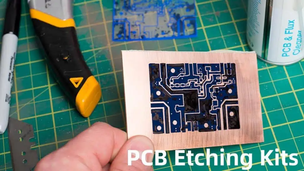
Toner Transfer Method
The toner transfer method is one of the quickest ways to produce a PCB in a lab setting.
Process Overview
- Print PCB layout on glossy paper
- Transfer toner to copper-clad board using heat and pressure
- Etch the board
- Drill holes
- Clean and prepare for component mounting
Pros and Cons
| Pros | Cons |
| Fast and simple | Limited resolution |
| Low equipment cost | Inconsistent results |
| Suitable for prototypes | Not ideal for fine-pitch components |
Photoresist Method
The photoresist method offers better precision but requires more specialized equipment.
Process Overview
- Apply photoresist to copper-clad board
- Print PCB layout on transparency
- Expose board to UV light through transparency
- Develop photoresist
- Etch the board
- Drill holes
- Clean and prepare for component mounting
Pros and Conss
| Pros | Cons |
| Higher precision | Requires UV exposure equipment |
| Consistent results | More time-consuming |
| Suitable for fine-pitch components | Higher material cost |
Step-by-Step Guide to Quick Double-Sided PCB Production
1. Design Phase
Circuit Design
- Create schematic diagram
- Convert schematic to PCB layout
- Optimize component placement and routing
- Add ground planes and power planes
- Include alignment marks for double-sided alignment
Design Verification
2. Preparing the Copper-Clad Board
- Cut the board to size
- Clean the copper surfaces thoroughly
- Apply photoresist or prepare for toner transfer
3. Transferring the PCB Layout
Toner Transfer Method
- Print the PCB layout on glossy paper (mirror image for bottom layer)
- Align and place the printed layout on the copper-clad board
- Apply heat and pressure using an iron or laminator
- Carefully remove the paper, leaving the toner on the copper
Photoresist Method
- Print PCB layout on transparency sheets
- Align transparency on photoresist-coated board
- Expose to UV light for the recommended duration
- Develop the photoresist using the appropriate chemical developer
4. Etching the Board
- Prepare etching solution (e.g., ferric chloride)
- Submerge board in etchant, agitating gently
- Monitor etching progress
- Rinse board thoroughly when etching is complete
5. Drilling Holes
- Use alignment marks to ensure proper registration
- Drill component holes and vias
- Clean the board to remove any debris
6. Through-Hole Plating (Optional)
For a true double-sided PCB, through-hole plating is necessary to connect both sides.
Quick Through-Hole Plating Methods
- Riveting: Use small copper rivets in vias
- Wire Bridging: Solder thin wires through vias
- Conductive Paint: Apply silver-based conductive paint in vias
7. Applying Solder Mask (Optional)
- Clean the board thoroughly
- Apply liquid solder mask or solder mask film
- Expose and develop solder mask (if using photoimageable type)
- Cure solder mask according to manufacturer’s instructions
8. Applying Silkscreen (Optional)
- Print component labels and markings on transfer paper
- Iron-on transfer or use acrylic paint and stencils
9. Final Preparation and Quality Check
- Perform visual inspection
- Check for shorts using a multimeter
- Clean the board one last time
Tips for Faster Production
- Optimize your PCB design for quick production (wider traces, larger clearances)
- Prepare all materials and equipment before starting
- Use pre-sensitized boards to save time on photoresist application
- Consider using spray-on etchant for faster and more even etching
- Invest in a small CNC drill for quicker and more accurate drilling
- Use alignment pins or a jig for double-sided alignment
Common Challenges and Solutions
| Challenge | Solution |
| Misalignment between layers | Use proper alignment marks and techniques |
| Overetching or underetching | Carefully monitor etching process and time |
| Poor toner transfer | Ensure proper heat and pressure application |
| Broken traces | Carefully inspect and repair with solder or conductive paint |
| Drill wandering | Use a drill press or CNC drill for accuracy |
Safety Considerations
- Always work in a well-ventilated area
- Wear appropriate personal protective equipment (PPE)
- Handle chemicals carefully and dispose of them properly
- Be cautious when using hot tools like irons or laminators
- Follow proper electrical safety practices when testing the PCB
Frequently Asked Questions (FAQ)
- Q: What’s the fastest method to produce a double-sided PCB in a lab? A: The toner transfer method is generally the fastest for producing a double-sided PCB in a lab setting. It requires minimal specialized equipment and can be completed in a few hours.
- Q: How can I ensure proper alignment between the top and bottom layers? A: Use alignment marks in your PCB design, and consider using alignment pins or a jig during the transfer process. For the photoresist method, you can use a double-sided UV exposure unit for perfect alignment.
- Q: What’s the quickest way to create through-hole connections in a lab-produced PCB? A: The fastest method is usually to solder thin wires through the vias, connecting the top and bottom layers. This technique, known as wire bridging, is quick and doesn’t require specialized plating equipment.
- Q: How can I improve the resolution of my lab-produced PCBs? A: To improve resolution, consider using the photoresist method instead of toner transfer. Also, ensure your transparency or printout is high quality, use fine-tipped markers for touch-ups, and carefully control the etching process.
- Q: Is it possible to produce multilayer PCBs quickly in a lab setting? A: While it’s possible, producing multilayer PCBs in a lab setting is significantly more complex and time-consuming than double-sided PCBs. For quick prototyping, it’s often more efficient to redesign the circuit for a double-sided board or use commercial PCB fabrication services for multilayer designs.