Advanced Circuit Solutions for Next-Generation Electronics
Our Multilayer HDI (High Density Interconnect) PCBs represent the cutting edge of printed circuit board technology, designed to meet the demanding requirements of today’s compact, high-performance electronic devices. These sophisticated boards utilize advanced manufacturing techniques to achieve unprecedented circuit density while maintaining superior electrical performance.
Key Features:
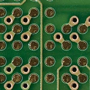
Ultra-High Circuit Density – HDI technology enables significantly more connections per unit area compared to traditional PCBs, with via-in-pad capabilities and microvias as small as 0.1mm diameter. This allows for complex routing in minimal space.
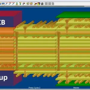
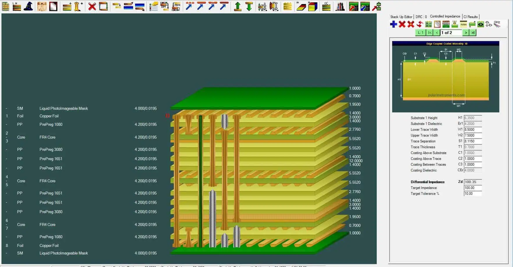
Advanced Layer Stack-up – Available in configurations from 4 to 20+ layers, with sequential lamination processes that enable blind and buried vias for optimal signal routing and space utilization.
Superior Signal Integrity – Shorter signal paths and reduced parasitic effects result in improved electrical performance, making these boards ideal for high-frequency applications up to millimeter-wave frequencies.
Miniaturization Excellence – Perfect for space-constrained applications where traditional PCB technology reaches its limits, enabling smaller form factors without compromising functionality.
Enhanced Thermal Management – Strategic via placement and advanced materials help dissipate heat more effectively, crucial for high-power density applications.
Applications:
- Smartphones and tablets
- Wearable electronics
- Medical devices and implants
- Automotive electronics
- Aerospace and defense systems
- IoT devices and sensors
- High-speed computing equipment
Technical Specifications:
- Line width/spacing: Down to 25/25 μm
- Via diameter: 0.1-0.15mm (microvias)
- Layer count: 4-20+ layers
- Board thickness: 0.4-3.2mm
- Impedance control: ±5% tolerance
- Material options: FR-4, Rogers, polyimide, and other advanced substrates
Quality Assurance: All HDI PCBs undergo rigorous testing including electrical testing, microsection analysis, and thermal cycling to ensure reliability in demanding applications. Our manufacturing processes are certified to ISO 9001, IPC Class 3, and automotive standards.
Why Choose Our HDI PCBs: With state-of-the-art manufacturing facilities and experienced engineering support, we deliver HDI solutions that push the boundaries of what’s possible in electronic design. Our expertise in advanced materials and processes ensures your products meet the highest performance standards while optimizing cost-effectiveness.
Transform your next-generation electronic designs with our Multilayer HDI PCB solutions – where innovation meets precision manufacturing.