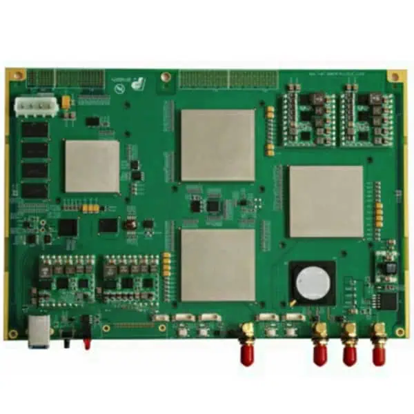
The hardware circuit part mainly adopts high-speed and large-capacity AD and FPGA to complete the functions of broadband and high-speed AD conversion and demodulation, high-efficiency decoding and so on. The hardware circuit mainly includes ultra-high-speed A/D conversion circuit, FPGA circuit, D/A conversion circuit, control circuit, interface between each part of the circuit and power supply circuit. The hardware circuit provides input data and processing resources for the software processing module, and completes high-speed digital demodulation and decoding under the unified coordination of the software.
Main indicators :
● Standard 6U board;
● 3 pieces of XC7VX690 high-performance FPGA;
● 1 piece of XC7K325T high-performance FPGA;
● 3.6GSPS high-speed sampling 14bits resolution ADC;
● 8xPCIE interface, USB3.0 interface.
High-speed and high-capacity Analog-to-Digital (AD) conversion coupled with FPGA-based demodulation is crucial in many advanced electronic systems, including software-defined radios, radar systems, and high-performance test and measurement equipment. Designing and manufacturing PCBAs for these applications requires careful consideration of various factors to ensure optimal performance, reliability, and manufacturability.
2. AD Converter Selection and Design Considerations
2.1 Selecting the Right AD Converter
- Choose an AD converter with appropriate resolution and sampling rate for your application.
- Consider factors such as Signal-to-Noise Ratio (SNR), Spurious-Free Dynamic Range (SFDR), and power consumption.
- Evaluate different AD architectures (e.g., SAR, pipeline, delta-sigma) based on your specific requirements.
2.2 Analog Front-End Design
- Implement proper anti-aliasing filters to limit the input signal bandwidth.
- Design a low-noise, high-bandwidth amplifier stage to condition the input signal.
- Consider using differential signaling to improve noise immunity and dynamic range.
2.3 Clock Distribution and Jitter Management
- Use low-jitter clock sources to minimize sampling uncertainties.
- Implement proper clock distribution networks with controlled impedance and minimal skew.
- Consider using clock buffers or PLLs for clock multiplication and distribution.
3. FPGA Selection and Design Considerations
3.1 Choosing the Right FPGA
- Select an FPGA with sufficient logic resources, DSP blocks, and memory for your demodulation algorithms.
- Consider power consumption and thermal management requirements.
- Evaluate the availability of high-speed transceivers for data interfacing if needed.
3.2 FPGA Configuration and Programming
- Implement a reliable configuration scheme (e.g., JTAG, SPI flash) for the FPGA.
- Consider security features such as bitstream encryption to protect your intellectual property.
- Design for in-system programmability to allow for firmware updates and reconfiguration.
3.3 FPGA-AD Interface Design
- Use high-speed LVDS or JESD204B interfaces for data transfer between AD converter and FPGA.
- Implement proper termination and impedance matching for high-speed signals.
- Consider using SerDes (Serializer/Deserializer) blocks for efficient data transfer.
4. PCB Design and Layout Considerations
4.1 Layer Stack-up and Impedance Control
- Design an appropriate layer stack-up with dedicated power and ground planes.
- Implement controlled impedance for high-speed traces using appropriate trace widths and spacings.
- Consider using high-speed PCB materials (e.g., Rogers, Megtron) for critical signal paths.
4.2 Signal Integrity and EMI Mitigation
- Use proper grounding and shielding techniques to minimize EMI and crosstalk.
- Implement guard traces or ground planes around sensitive analog signals.
- Use differential pairs for high-speed signals and ensure proper length matching.
4.3 Power Integrity and Distribution
- Design robust power distribution networks with low impedance and minimal noise.
- Use decoupling capacitors near power pins of ICs to reduce noise and maintain signal integrity.
- Consider using power planes with stitching vias for improved current distribution.
5. Thermal Management
- Implement proper thermal management solutions for heat-generating components (e.g., FPGA, voltage regulators).
- Use thermal simulations to identify potential hotspots and optimize component placement.
- Consider using heat sinks, thermal vias, or forced-air cooling for high-power designs.
6. Manufacturing Considerations
6.1 Design for Manufacturing (DFM)
- Follow DFM guidelines to ensure producibility and yield.
- Consider factors such as minimum trace widths, via sizes, and solder mask clearances.
- Use fiducial marks for accurate component placement during assembly.
6.2 Assembly Process
- Choose appropriate surface finish (e.g., ENIG, immersion silver) for reliable soldering.
- Consider using stencil designs optimized for fine-pitch components.
- Implement proper reflow profiles for lead-free soldering processes.
6.3 Testing and Quality Control
- Design for testability by including test points and implementing boundary scan capabilities.
- Develop comprehensive functional test procedures to verify system performance.
- Implement in-circuit testing (ICT) or flying probe testing for manufacturing defect detection.
7. Firmware Development and System Integration
- Develop efficient FPGA firmware for demodulation algorithms using HDL (e.g., VHDL, Verilog).
- Implement proper interfaces between FPGA and other system components (e.g., microcontrollers, memory).
- Consider using high-level synthesis (HLS) tools for complex algorithm implementation.
8. Conclusion
Designing and manufacturing high-speed and high-capacity AD and FPGA conversion and demodulation PCBAs requires a multidisciplinary approach, combining expertise in analog and digital design, signal integrity, PCB layout, and manufacturing processes. By carefully considering the factors outlined in this guide, engineers can create robust and high-performance systems that meet the demanding requirements of modern electronic applications.