Unlock Next-Generation Circuit Density with Professional HDI PCB Solutions
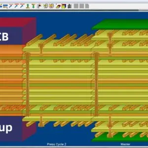
Our Any Layer HDI (High Density Interconnect) PCBs represent the pinnacle of advanced circuit board technology, delivering unprecedented miniaturization capabilities for today’s most demanding electronic applications. Engineered with microvias, buried vias, and blind vias throughout multiple layers, these boards enable complex routing in compact form factors that traditional PCBs simply cannot achieve.
Key Features
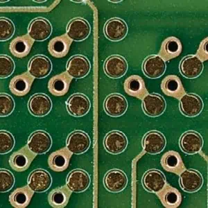
Advanced Via Technology: Featuring microvias as small as 0.1mm diameter with precise laser drilling, our HDI boards support via-in-pad configurations and stacked microvia structures for maximum routing density.
Multi-Layer Flexibility: Available in configurations from 4 to 20+ layers with any-layer interconnect capability, allowing signal routing between any combination of layers for optimal design freedom.
Superior Signal Integrity: Controlled impedance design with tight tolerances (±5%) ensures excellent high-frequency performance, making these boards ideal for RF applications, high-speed digital circuits, and sensitive analog designs.
Exceptional Miniaturization: Achieve up to 75% size reduction compared to conventional PCBs while maintaining full functionality, perfect for smartphones, wearables, medical devices, and aerospace applications.
Technical Specifications
- Layer Count: 4-20+ layers with sequential build-up
- Minimum Trace Width: 0.075mm (3 mil)
- Minimum Via Size: 0.1mm diameter microvias
- Board Thickness: 0.4mm to 3.2mm
- Aspect Ratio: Up to 12:1 for through holes
- Surface Finish: HASL, ENIG, OSP, or Immersion Silver
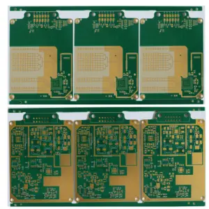
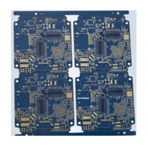
Applications
Perfect for cutting-edge electronics including 5G telecommunications equipment, IoT devices, automotive electronics, medical implants, and high-performance computing systems where space constraints and signal integrity are critical.
Manufacturing Excellence: Built using state-of-the-art sequential lamination processes with rigorous quality control at every step. Full electrical testing and AOI inspection ensure 99.5% yield rates and reliable performance in mission-critical applications.
Transform your next project with HDI technology that pushes the boundaries of what’s possible in electronic design.