In printed circuit board (PCB) design, the term “net” refers to electrical nodes or points that need to be connected together in the circuit layout. Nets represent the logical connectivity defined in the schematics. All pins and ports that are connected together electrically belong to the same net.
PCB layout involves identifying all nets and then connecting them on the board layout using copper traces and vias while meeting design rules. Understanding the role of nets is key for successful board layout and manufacturing. This article provides an in-depth overview of PCB nets – what they are, how they are specified, routing considerations, and more.
What is a Net in PCB Layout?
A net is defined as a collection of electrically connected nodes or points which need to be joined with copper tracking to make them a single signal or potential point. Some key points:
- Nets represent logical rather than physical connections.
- All component pins part of a net must be at same electrical potential.
- A net may have 2 or more component pins/pads connected to it.
- Multi-point connections define nets – e.g. common power or ground nets.
- Nets get mapped to physical PCB copper tracking during layout.
- Each net is identified by a unique name or number.
Essentially, nets list which pins and ports on the schematic are meant to be connected electrically on the PCB layout. Correct netlist definition is crucial.
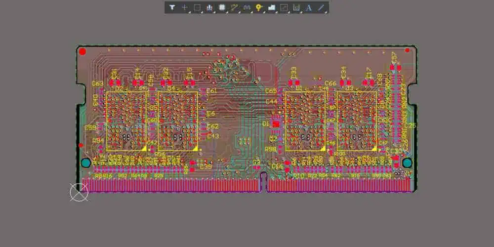
Example of multiple PCB component pins belonging to a common net
Why Specify Nets in PCB Layout?
Defining nets serves several important purposes:
- Captures logical connectivity – Nets represent schematic connectivity requirements that must be achieved with physical layout.
- Enables ERC – Electrical rules checking verifies all nets are properly connected with no opens or shorts.
- Facilitates autorouting – Routers can use net info to automatically connect defined nets.
- Allows design validation – Netlist can be cross-checked against schematics for correctness.
- Aids manufacturability – Unconnected nets highlight problems for assembly and test.
- Speeds fault isolation – Confirms if bad joints/breaks are causing net opens.
In summary, identifying nets is key to translating the electrical connectivity model into the physical PCB layout correctly while meeting design rules.
Specifying Nets in CAD Tools
PCB layout CAD tools like Altium Designer provide powerful support for defining, managing and routing nets spanning multiple component pins. Some key features related to nets:
Net Identifier
A unique name or number assigned to each net. Can be auto-generated or user-defined. Examples: NetA, Power, +5V, Audio_Out etc.
Net Scope
The logical boundary or extent of a net. Allows optimization of routing boundaries.
Net Classes
Nets can be grouped into classes with shared rules like routing widths, spacing, via styles etc.
Net Tie
An electrical connection defined between two different nets that forces them to be shorted.
Power Planes
Entire plane layers can define nets like GND or VCC, allowing connections through vias.
Differential Pairs
Grouping differential signal nets enables linked length-matching routing.
Net Properties
Nets can have attributes like drive current, impedance, delay etc. attached for analysis.
Proper specification of these net parameters in the PCB CAD system is needed for robust ERC checks, autorouting and design validation against schematics.
Guidelines for Naming Nets
When defining custom net names, following naming conventions helps keep netlists well-organized and easy to understand:
- Keep names short but meaningful e.g. “PWREN” instead of “POWERENABLE”.
- Use consistent prefixes for net types e.g. “SIG_” for signals, “PWR_” for power.
- Avoid using non-alphanumeric characters in names to prevent tool issues.
- Use uppercase letters to make names stand out.
- Include pin numbers if needed for clarity e.g. “CLK2”
- Use sequential numbers for grouped nets e.g. “D0-D7”.
- Add relevant functional descriptions e.g. “LED_STATUS”
- Designate I/O signals clearly e.g. “USB_D+”
Intelligent net naming strategies help identify the signal or connection purpose at a glance during layout routing and inspection.
Cross-Probing to Schematics
Modern PCB CAD tools allow cross-probing from PCB layout to schematics to quickly understand net connectivity and context. When clicking a net in layout, the associated pins/nodes in the schematics are automatically highlighted.
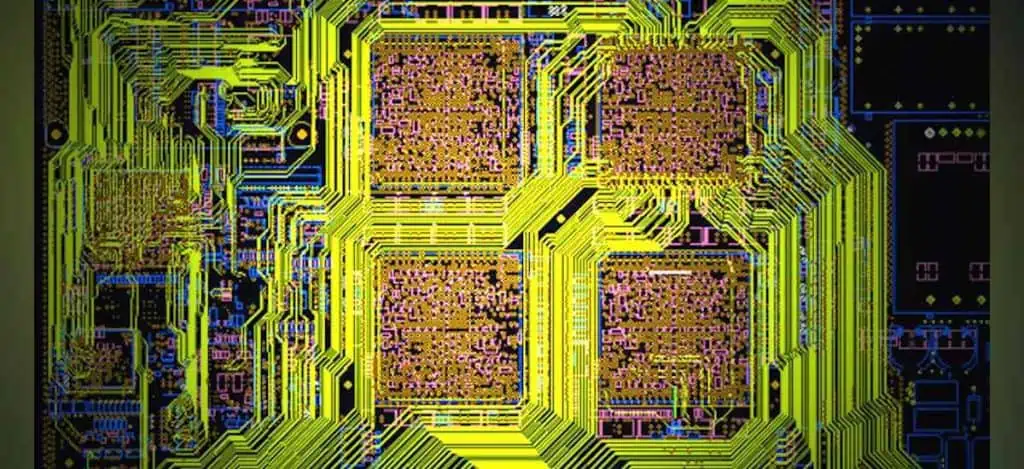
Visual cross-probing from PCB layout net to schematic net highlights associated pins
This very useful feature allows layout designers to instantly visualize which component pins belong to a net. It aids in layout decisions like optimal component placement and routing paths to maintain net integrity.
Routing Considerations for Nets
When laying out nets using copper tracks and vias, several factors must be considered:
- Priority – Route critical nets like clocks and power first.
- Topology – Use point-to-point, daisy chains or tree routing as appropriate.
- Impedance – Match trace geometry to required impedance.
- Currents – Size tracks based on expected current.
- Length Matching – Equal net lengths for clocks, differential signals etc.
- Crosstalk – Provide adequate spacing between nets.
- Stackup – Use correct signal layers.
- Shielding – Shield noisy traces using ground planes.
- Terminations – Add resistors at line ends when needed.
- Vias – Minimize/avoid vias on critical nets.
Applying these rules during layout ensures nets get implemented with the desired signal quality and integrity.
Best Practices for Defining Nets
Follow these guidelines when specifying nets for a PCB layout:
- Capture all component-to-component connections as nets – avoid assuming implied connections.
- Group multiple pins of IC/connectors into nets representing bussed signals.
- Review the netlist against schematics and datasheets thoroughly to prevent omissions.
- Define power and ground nets carefully for power integrity analysis.
- Use named nets rather than direct component-to-component connections for clarity.
- Re-use common nets rather than defining duplicates to minimize errors.
- Create differential pair and bus nets to simplify routing and constraints.
- Specify net classes and routing rules based on signal types – clock, data, analog etc.
Well-defined nets are crucial for achieving smooth PCB layout implementation and avoiding manufacturing issues due to incorrect copper connectivity.
Conclusion
In summary, PCB nets provide the vital link between the logical connectivity in an electrical schematic and the physical layout topology on the board. Defining nets correctly and routing them according to electrical and layout constraints is key to creating fabrication-ready PCB artwork. CAD systems simplify net handling with features like auto-naming, cross-probing, classes and differential pairs. With the growth in design complexity, net management has become critical for layout success. Understanding every aspect of PCB nets is essential for both design engineers and layout specialists.
FAQ
Here are some common questions about nets in PCB layout:
Q1: Can two nets have the same name in a PCB layout?
No, each defined net must have a unique name to avoid ambiguity during layout. Identical names would lead to connection errors.
Q2: How are net names transferred from schematic capture to PCB layout?
The netlist, which maps net names to component pins, is passed from schematics to PCB layout either as a file or through direct tool integration.
Q3: Can net scope constrain routing to a particular PCB region?
Yes, the scope can define a keep-in or keep-out region for a net’s routing to optimize layout.
Q4: What is a net tie?
A net tie intentionally shorts two nets together by defining a connection between them. It is useful for tying power/ground nets.
Q5: Can simulation use the netlist from PCB layout?
Yes, the layout netlist can be used for signal integrity and power integrity analyses using simulators.