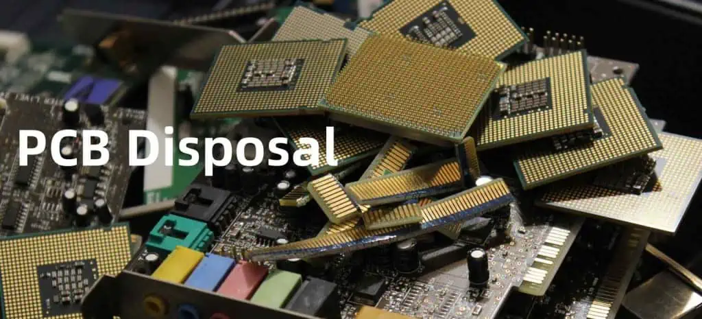
Printed circuit boards (PCBs) are essential components of almost every electronic device we use today. However, at the end of their useful life, disposing PCB waste requires special attention owing to the complex mix of metals and hazardous compounds present on boards.
This article explores recommended techniques for responsible PCB waste management across various categories:<h2>Contents</h2>
- Overview of PCB Waste Generation
- PCB Disposal Challenges
- Best Practices for PCB Waste Management
- Reuse
- Recycling and Recovery
- Incineration
- Landfilling
- Legislations Governing PCB Disposal
- Role of Standards in PCB Waste Processing
- Conclusion
- FQA on PCB Disposal
Overview of Global PCB Waste Generation
Printed circuit boards are indispensable components across computers, communication infrastructures, transport systems, home appliances and consumer electronics worldwide. The global PCB industry reached a size exceeding $72.6 billion in 2021 supporting an ever-growing range of complex electronic devices.
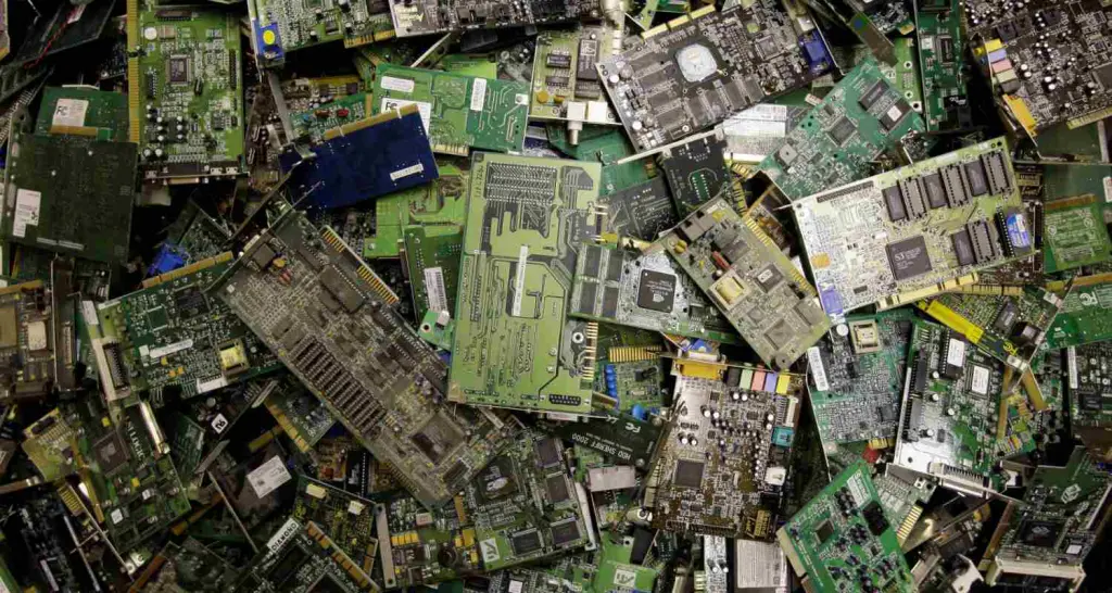
However, the flip side is the massive amount of waste PCBs being discarded annually across the world. According to estimates, the total e-waste generation consisting of end-of-life electronic products will touch 75 million metric tons (MMT) by 2030, the weight of over 125 Empire State Buildings!
Another worrying insight is that only 20% of global e-waste is documented to be collected and recycled. The remaining waste accumulates in landfills, gets incinerated, or exported illicitly. Such reckless dumping causes substantial harm from the release of dangerous substances especially from PCB waste.
Table showing projected global e-waste generation:
| Year | Estimated E-Waste Generated (MMT) |
|---|---|
| 2019 | 53.6 MMT |
| 2020 | 57.4 MMT |
| 2030 | 75 MMT (projected) |
This highlights the urgent need to implement responsible and sustainable e-waste management practices targeting PCB waste recycling and recovery.
Next, let’s analyze the key challenges in PCB disposal and essential best practices manufacturers must adopt.
PCB Disposal Challenges
PCB waste poses complex disposal risks due to:
Hazardous Substances Composition
Printed circuit boards contain over 60 metals and metalloids including lead, cadmium, chromium, mercury, beryllium, and flame retardants. Such toxic substances can contaminate soil and groundwater if landfilled.
Difficult Separation and Collection
E-waste is difficult to systematically collect and transportation proves costly owing to the presence of hazardous fractions mixed with benign metals. Sorting different material fractions require advanced processing.
Unsafe Treatment in Unorganized Sector
In emerging economies, the unorganized sector handles 80% of e-waste including PCBs. Uncontrolled recycling techniques like acid leaching, open burning or landfilling create severe environmental and health issues.
Lack of Policy Implementation
There is inadequate regulation and enforcement checks on illegal waste trade and substandard treatment practices especially in developing countries which import bulk discarded electronics from the developed world.
However, adopting best practices and circular economy models for PCB waste management can help overcome these barriers across the industry value chain while extracting economic value from end-of-life boards.
Best Practices for PCB Waste Management
Responsible PCB waste management integrates multiple approaches from reuse to recycling and energy recovery. The foremost priorities as per WEEE (Waste Electrical and Electronic Equipment) directives are:
Reuse – Extend lifespan by reselling to new users
Recycle & Recover – Recover metals, polymers, glass; dispose non-recyclables responsibly
Energy Recovery – Incinerate waste in controlled facilities
Disposal – Landfill restricted fractions in designated sites
The choice depends upon composition, available processing infrastructure and regulations. Let’s examine these strategies involving PCB waste.
1. Reuse
PCBs comprising functioning components can be directly reused via repair, refurbishment or remanufacturing in different applications. Testing, cleaning and minor rework helps restore used PCBs supporting the circular economy. Advances in remanufacturing technology enables upgrading circuitry and durability.
Certified public reuse platforms now facilitate the sale of previously used electronics and PCB modules. They evaluate material quality to maximize utilization lifespan across second users. While reuse helps extend value, most waste PCBs ultimately require material recovery.
2. Recycling and Recovery
Recycling involves specialized processes for dismantling, separation, shredding, and smelting to extract constituent metals, solder, polymers and glass powder from waste PCBs.<h3>Key stages comprise:</h3>
Manual dismantling – Remove reusable components
Size reduction – Shredding andgrinding improves material liberation and handling
Mechanical separation – Magnetic, density separation extracts ferrous and non-ferrous metals
Hydrometallurgical recovery – Leaches metals using chemicals/solvents
Smelting and refining – Recover high purity metals mainly Cu, Al, Sn, Pb, Ni, Au
Plastic recovery – Clean/grind thermoset polymers into filler material
Such recycling enables efficient material recovery beyond 50% from waste PCBs with steady improvements in separation technology. Ensuring minimal toxic emissions into soil, water and air is vital across these processes.
3. Incineration
Waste with no scope for material recovery gets incinerated to reduce volume (upto 90% volume reduction) while also generating electricity. Modern incinerators feature air pollution control systems with specific gas treatment equipment.
Several countries now have dedicated waste to energy (WTE) bio-mass plants suitable for treating specific electronic waste fractions containing wood, plastics etc. However, burning e-waste openly or in inappropriate facilities remain banned owing to high toxicity. While controlled incineration reduces landfills, the focus still lies on maximizing product reuse and recycling over energy recovery.
4. Landfilling
Landfills serve as the last resort for restricted residual material like fiberglass and other inert e-waste constituents not viable for recovery. Stable toxic residues get specially handled and capped with layers of impermeable liners within landfills to minimize groundwater contamination risks.
Sustainable landfill management demands systematic storage, sealing barriers and prolonged aftercare post closure. For instance, Germany mandates a 30 year minimum aftercare monitoring period for municipal landfills receiving PCB waste disposal. With specialized handling and containment measures, landfills provide the final containment step as per EU’s waste framework model.
Legislations Governing PCB Disposal
Several regions now implement dedicated regulations around disposal, transport and treatment for end-of-life electronics containing PCB waste.
Europe – Waste Electrical and Electronic Equipment (WEEE) directive
USA – Resource Conservation and Recovery Act (RCRA); Toxic Substances Control Act
Japan – Law for Promotion of Effective Utilization of Resources
These define collection targets, restricted substances limits, and phase-out timelines for toxic materials like lead, mercury, cadmium and hexavalent chromium now banned in manufacturing. Developing nations also enact parallel e-waste rules aligned to the above global guidelines.
Furthermore, regulations necessitate permits/licenses for authorized recycling facilities meeting environmental compliances. Approved Treatment, Storage and Disposal Facilities (TSDFs) help implement responsible PCB disposal and combat illegal waste exports. Expanding these regulated recycling infrastructures particularly across Asia and Africa remains vital to manage rapidly rising waste volumes.
Role of Standards in PCB waste processing
Voluntary consensus standards provide consistent protocols and control criteria across PCB waste management operations namely –
- Collection – ANSI/IICRC S500 Standard for Professional Water Damage Restoration outlines waste sorting categories to segregate PCB containing electronics.
- Transportation – Responsible e-waste transportation protocols defined under R2 and RIOS standards minimize environmental and health risks.
- Recycling – R2 Standard for Responsible Recycling of E-waste controls material processing via environmental, health and safety management specifications.
- Incineration and Landfills – Relevant standards monitor air emissions, ash disposal limits, leachate quality parameters etc. to improve PCB incineration and landfill disposal safety.
Such standards mature waste management ecosystems once widely adopted by industry operators and local municipalities. Voluntary adoption even drives innovations in sustainable PCB disposal technology.
Conclusion
In summary, PCB waste requires coordinated progress across policy definition, compliant infrastructure advancements and voluntary standardization for extracting maximum value while also mitigating ecological risks. The priority action areas involve:
♻️ Improving collection systems and recycling rates
♻️ Expanding regulated recycling capacities by permitting more treatment facilities
♻️ Advancing separation techniques targeting improved material purity and recovery
♻️ Encouraging product-centric eco-designs supporting reusability and recyclability
♻️ Monitoring disposal procedures via integrated electronics supply chains
♻️ Implementing global circular economy models for electronic waste comprising PCBs
With electronics getting increasingly interconnected across critical functions, managing soaring volumes of complex end-of-life products demands urgent priority to transition towards smart, ethical and efficient PCB waste management.
FQA on PCB Disposal
What percentage of PCB waste gets recycled globally?
As per estimates, only around 30% of end-of-life PCBs are documented to be responsibly collected and recycled worldwide as of 2020. Bulk fractions of PCB waste still get incinerated or landfilled due to processing complexity and inadequate recycling infrastructure currently.
Does PCB waste require special handling measures?
Yes, owing to presence of heavy metals and brominated flame retardants, PCB waste warrants special safety precautions during handling, storage, transportation and treatment. Workers need adequate protective gear while manual dismantling given toxicity risks via dust inhalation, cuts or burns.
What alternative technology shows promise for improved PCB recycling rates?
Emerging pyrolysis techniques using high temperature decomposition in the absence of oxygen can selectively separate complex e-waste. Pyrolysis optimizes PCB recycling by lower energy usage and better brominated flame retardant capture compared to incineration. However, the process requires further commercial scale-up.
Can good product design enable easier PCB recycling?
Yes, designing hardware focused on extended lifespan along easier disassembly, repair and modular upgrades aids PCB circularity. Eliminating toxic materials and using more easily separable component joining techniques (like snap fits) facilitates cleaner material segregation from waste PCBs as well.
Do PCBs get exported abroad for treatment from developed countries?
While legally prohibited, investigations reveal that discarded electronics from the EU, USA and Japan rampantly get labeled as second-hand goods for re-export into poorer nations where unregulated backyard operations use hazardous recycling methods generating immense pollution and health issues. Global cooperation is vital to curb this unauthorized waste trade.