Advanced PCB Manufacturing: Up to 100 layers. Specializing in R&D and high-complexity designs. Contact us for cost estimation.
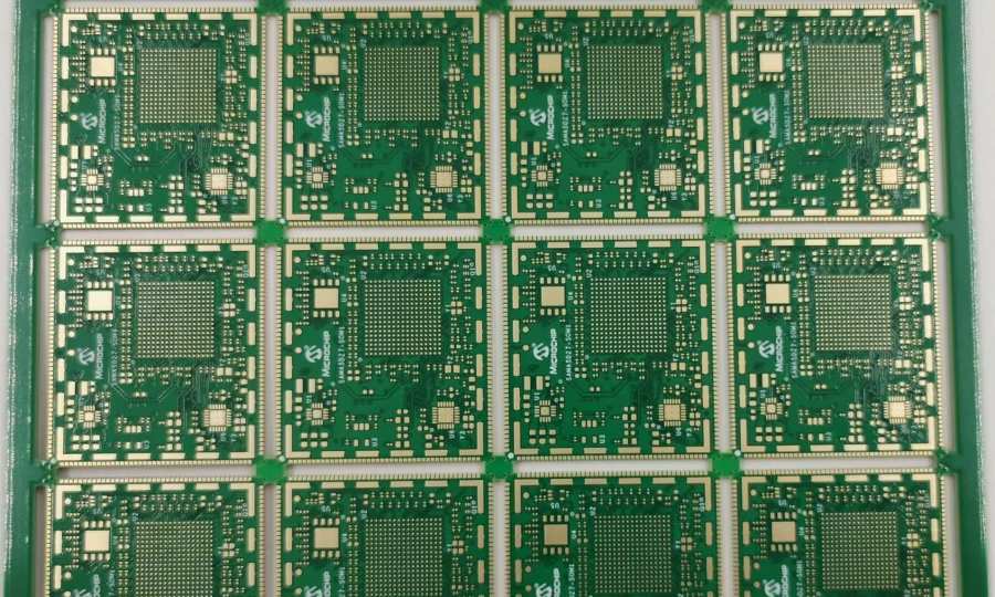
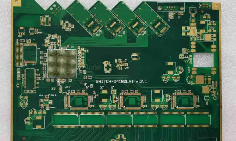
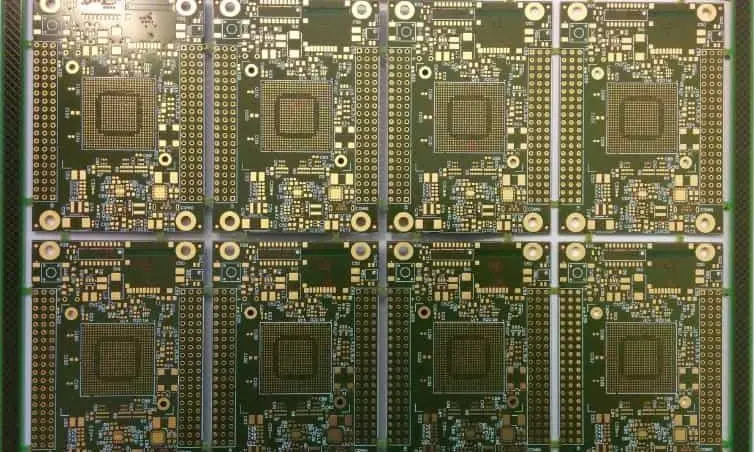
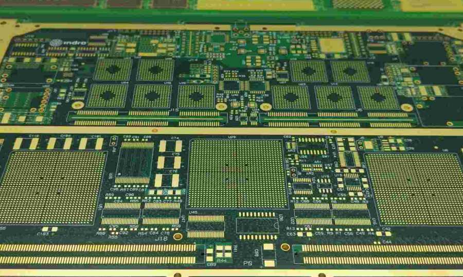
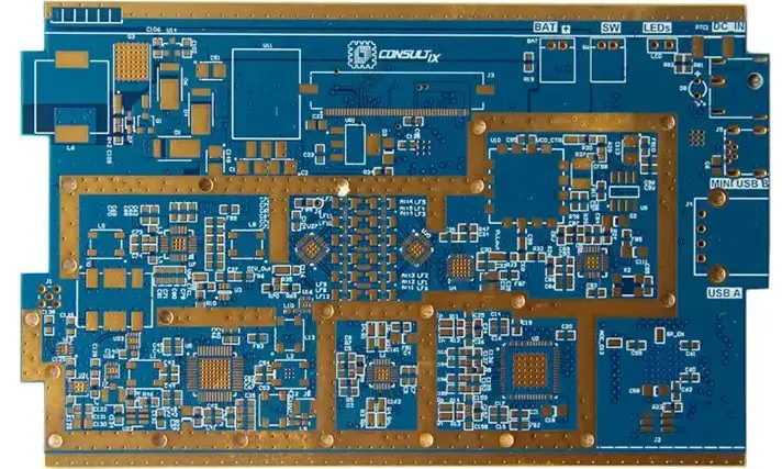
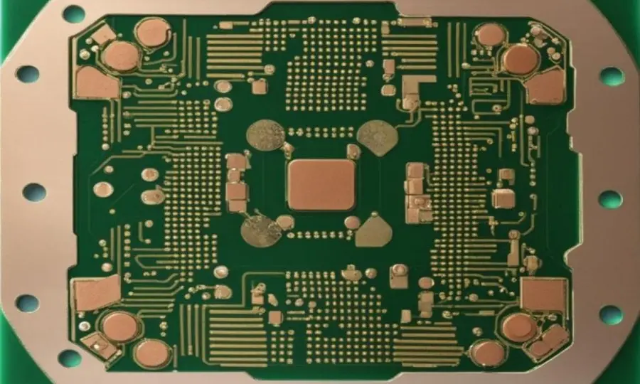
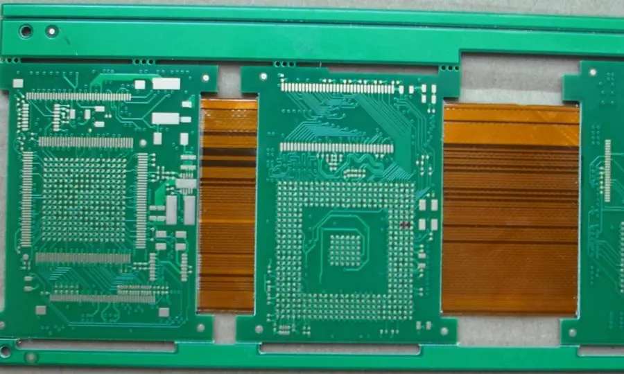
A multilayer PCB represents one of the most significant advances in printed circuit board technology, enabling complex electronic designs in compact form factors. Unlike single or double-layer boards, a multilayer PCB consists of three or more conductive copper layers separated by insulating dielectric materials, all laminated together into a single, cohesive board structure.
The evolution of multilayer PCB design has been driven by the relentless miniaturization of electronic devices and the increasing complexity of modern circuits. From smartphones and laptops to automotive control systems and industrial automation equipment, multilayer PCBs form the backbone of virtually every sophisticated electronic system in use today.
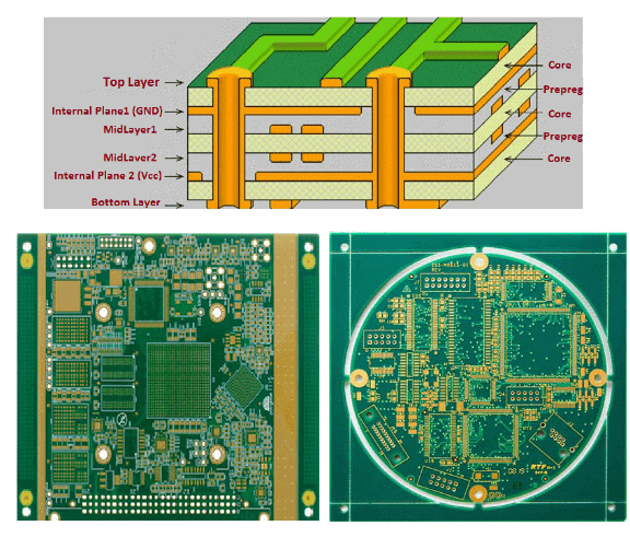
Every multilayer PCB is built using a precise stack-up of alternating conductive and insulating layers. The basic structure includes:
The manufacturing process involves laminating these materials under high temperature and pressure, creating a monolithic board structure with excellent mechanical and electrical properties.
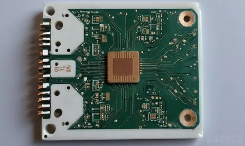
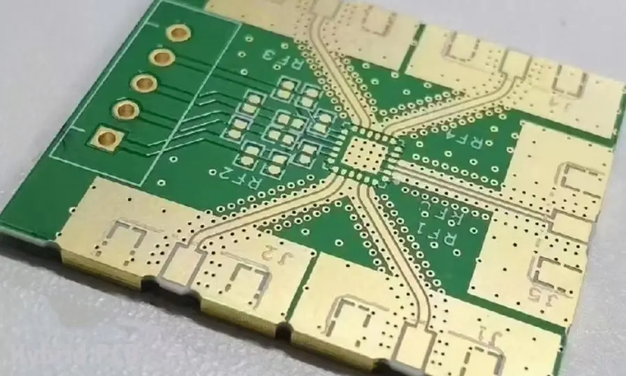
The primary advantage of multilayer PCB technology lies in its ability to pack more functionality into smaller spaces. By routing traces on internal layers, designers can significantly reduce board footprint while maintaining or even improving electrical performance. This space efficiency is crucial for portable electronics, medical devices, and automotive applications where size constraints are paramount.
Multilayer PCBs offer superior electrical characteristics compared to their single or double-layer counterparts:
The availability of multiple routing layers provides unprecedented design flexibility, enabling:
| Interface | Type | Target Ω | Tolerance | Typical Stack |
|---|---|---|---|---|
| USB 2.0 | Differential | 90Ω | ±10% | 5mil/5mil/4mil H |
| USB 3.0/3.1 | Differential | 90Ω | ±7% | 4mil/4mil/3.5mil H |
| PCIe Gen3/4 | Differential | 85Ω | ±10% | 4.5mil/5mil/4mil H |
| HDMI 1.4/2.0 | Differential | 100Ω | ±10% | 4mil/6mil/4mil H |
| DDR4 | Single-ended | 40Ω | ±10% | 6mil/4mil H |
| Ethernet 10G | Differential | 100Ω | ±10% | 4mil/5mil/3.5mil H |
| Parameter | Standard | Advanced | HDI |
|---|---|---|---|
| Min Trace Width | 5 mil (127µm) | 4 mil (102µm) | 3 mil (76µm) |
| Min Trace Spacing | 5 mil (127µm) | 4 mil (102µm) | 3 mil (76µm) |
| Min Via Diameter | 0.3mm | 0.2mm | 0.1mm |
| Min Via Pad | 0.6mm | 0.45mm | 0.25mm |
| Min Annular Ring | 0.15mm | 0.1mm | 0.075mm |
| Aspect Ratio (Via) | 8:1 | 10:1 | 12:1 |
| PTH to Trace | 10 mil | 8 mil | 6 mil |
| Via to Via | 8 mil | 6 mil | 5 mil |
| Application | Recommended Material | Key Property | Frequency Range |
|---|---|---|---|
| General Consumer | FR-4 Standard | Cost-effective | < 1 GHz |
| Industrial/Automotive | FR-4 High Tg / 370HR | High reliability | < 3 GHz |
| High-Speed Digital | Megtron 6 / I-Speed | Low loss, stable Dk | 5-25 GHz |
| RF/Microwave | Rogers RO4000 Series | Very low loss | > 10 GHz |
| mmWave/5G | Rogers RO3003/RT5880 | Ultra-low loss | > 30 GHz |
| Flexible Circuits | Polyimide (Kapton) | Flexibility | < 10 GHz |
The standard 4-layer PCB stack-up follows a proven arrangement:
This configuration provides an excellent balance between functionality and cost, making 4-layer boards the most popular choice for many applications.
When designing a 4-layer multilayer PCB, several key factors must be considered:
Layer Assignment Strategy: Assign high-speed and critical signals to the top and bottom layers, keeping them as short as possible. Use the internal planes for power distribution and signal return paths.
Via Management: Minimize via usage to reduce manufacturing costs and potential reliability issues. When vias are necessary, ensure proper placement to maintain signal integrity.
Power Distribution: Design robust power and ground networks using the internal planes. Consider copper pour techniques and strategic via placement for optimal current flow.
4-layer PCBs excel in applications such as:
However, they may be insufficient for highly complex designs with numerous power domains or extensive high-speed signaling requirements.
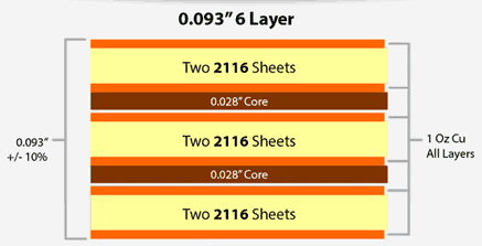
6-layer multilayer PCB designs offer greater flexibility with multiple stack-up possibilities:
Configuration 1: Signal-Ground-Signal-Signal-Power-Signal Configuration 2: Signal-Ground-Signal-Power-Signal-Signal Configuration 3: Signal-Ground-Power-Signal-Ground-Signal
Each configuration serves different design requirements, with the choice depending on signal density, power distribution needs, and EMI considerations.
The additional layers in a 6-layer multilayer PCB provide significant advantages:
Symmetric Stack-up: Maintain mechanical balance by using symmetric layer arrangements to prevent board warping during manufacturing and operation.
Controlled Impedance: Calculate and verify trace impedances for all signal layers, considering the dielectric properties and layer spacing.
Thermal Management: Utilize internal copper planes as heat spreaders, particularly important for high-power applications.
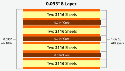
8-layer multilayer PCB designs represent the pinnacle of complexity for most commercial applications. Typical stack-up arrangements include:
High-Performance Configuration:
This configuration provides excellent signal integrity with multiple reference planes and optimized power distribution.
Layer Planning: Carefully plan layer usage to optimize signal routing and minimize electromagnetic interference. Group related signals on the same layers and provide appropriate reference planes.
Power Domain Separation: Use different internal layers for various power domains, ensuring proper isolation and filtering between voltage rails.
High-Speed Signal Management: Dedicate specific layers to high-speed signals with carefully controlled impedances and minimal layer changes.
8-layer boards require precise manufacturing processes:
Regardless of layer count, certain principles apply to all multilayer PCB designs:
Trace Width Calculations: Use industry-standard formulas to calculate minimum trace widths based on current carrying requirements and temperature rise limitations.
Via Design: Implement appropriate via sizes and drill-to-land ratios to ensure manufacturing reliability and electrical performance.
Component Placement: Optimize component placement to minimize trace lengths and facilitate efficient routing across multiple layers.
Electromagnetic compatibility is crucial in multilayer PCB design:
Multilayer PCB costs increase with layer count, making cost optimization essential:
Panel Utilization: Maximize board per panel to reduce per-unit costs Standard Materials: Use industry-standard materials and thicknesses when possible Via Optimization: Minimize blind and buried vias, which add significant cost Testing Requirements: Balance electrical testing needs with cost constraints
Develop strong relationships with PCB manufacturers who specialize in multilayer technology. Early engagement in the design process can identify cost-saving opportunities without compromising performance.
Inadequate thermal planning can lead to performance degradation and reliability problems:
Solution: Implement thermal vias to transfer heat between layers and use copper pours as heat spreaders.
Poor power distribution network design causes voltage fluctuations and system instability:
Solution: Design robust power and ground networks with appropriate decoupling capacitor placement and low-impedance paths.
Improper impedance control and poor layer transitions create signal quality issues:
Solution: Use controlled impedance design techniques and minimize unnecessary layer changes.
The multilayer PCB industry continues to evolve with several key trends:
HDI (High Density Interconnect): Increasing adoption of microvias and sequential build-up technology for ultra-compact designs.
Embedded Components: Integration of passive components within the PCB structure to further reduce size and improve performance.
Advanced Materials: Development of new dielectric materials with improved electrical and thermal properties.
Growth markets driving multilayer PCB innovation include:
Mastering multilayer PCB design requires understanding the complex interplay between electrical performance, mechanical constraints, and manufacturing capabilities. Whether designing 4, 6, or 8-layer boards, success depends on careful planning, adherence to design rules, and close collaboration with manufacturing partners.
The future of multilayer PCB technology promises even greater integration and performance capabilities. Designers who master these fundamentals will be well-positioned to tackle the increasingly complex challenges of modern electronic system design.
By following the guidelines and best practices outlined in this comprehensive guide, engineers can create robust, reliable multilayer PCB designs that meet the demanding requirements of today’s electronic systems while remaining cost-effective and manufacturable.
The evolution of multilayer PCB technology continues to enable the next generation of electronic innovations, from ultra-compact consumer devices to mission-critical industrial systems. Understanding these design principles ensures successful implementation of complex multilayer PCB projects in 2025 and beyond.