The evolution of Printed Circuit Board (PCB) manufacturing has seen significant advancement with the introduction of laser exposure technology. This revolutionary approach has transformed the traditional PCB production process, offering enhanced precision, improved efficiency, and superior quality output. This comprehensive article explores how laser exposure machines are revolutionizing the PCB industry and making the manufacturing process more efficient.
Understanding Laser Exposure Technology
Basic Principles
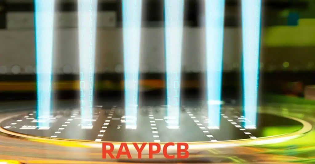
Laser exposure technology utilizes precise laser beams to directly image circuit patterns onto photoresist-coated PCB substrates. This technology eliminates the need for traditional photomasks and significantly reduces the complexity of the exposure process.
Key Components
| Component | Function | Impact on Efficiency |
| Laser Source | Pattern generation | High precision, fast processing |
| Optical System | Beam focusing and steering | Accurate pattern placement |
| Control System | Process management | Automated operation |
| Scanning System | Pattern distribution | Uniform exposure |
| Cooling System | Temperature regulation | Stable operation |
Advantages of Laser Exposure in PCB Manufacturing
Technical Benefits
1. Precision and Accuracy
| Parameter | Traditional Method | Laser Exposure | Improvement |
| Line Width | ±25μm | ±5μm | 80% better |
| Registration | ±50μm | ±10μm | 80% better |
| Edge Definition | ±15μm | ±3μm | 80% better |
| Layer Alignment | ±30μm | ±7μm | 77% better |
2. Production Speed
| Board Size | Traditional Exposure | Laser Exposure | Time Saved |
| Small (4″x6″) | 45 seconds | 15 seconds | 67% |
| Medium (8″x10″) | 90 seconds | 25 seconds | 72% |
| Large (12″x18″) | 180 seconds | 40 seconds | 78% |
Economic Benefits
Process Optimization
Workflow Improvements
- Digital workflow integration
- Reduced manual intervention
- Real-time quality control
- Automated correction systems
Production Parameters
| Parameter | Setting Range | Optimal Value | Impact on Quality |
| Laser Power | 1-5W | 3W | High |
| Scan Speed | 100-500mm/s | 300mm/s | Medium |
| Focus Distance | 10-30mm | 20mm | Critical |
| Resolution | 1200-4800dpi | 2400dpi | High |
Advanced Features and Capabilities
Multi-layer Processing
| Layer Type | Special Requirements | Processing Time |
| Inner Layer | High registration | 20-30 seconds |
| Outer Layer | Fine line capability | 25-35 seconds |
| Solder Mask | Precise alignment | 30-40 seconds |
| Legend | High contrast | 15-25 seconds |
Automation Features
Smart Functions
- Auto-alignment
- Pattern recognition
- Error detection
- Real-time adjustment
Quality Control and Monitoring
Quality Metrics
| Metric | Standard Range | Acceptable Deviation |
| Pattern Accuracy | ±5μm | ±2μm |
| Surface Uniformity | 95-100% | -2% |
| Edge Quality | 90-95% | -3% |
| Registration | ±7μm | ±3μm |
Process Monitoring
Real-time Parameters

| Parameter | Monitoring Method | Update Frequency |
| Laser Power | Direct measurement | Every 0.1s |
| Beam Position | Optical sensors | Every 0.05s |
| Temperature | Thermal sensors | Every 1s |
| Air Quality | Particle counters | Every 5s |
Environmental Impact
Energy Efficiency
| Process Stage | Traditional Power Usage | Laser System Power Usage | Savings |
| Startup | 5000W | 2000W | 60% |
| Operation | 3500W | 1500W | 57% |
| Standby | 1000W | 300W | 70% |
Material Conservation
Reduced Waste
| Material Type | Traditional Waste | Laser System Waste | Reduction |
| Photoresist | 15-20% | 5-8% | 60% |
| Chemistry | 25-30% | 10-12% | 60% |
| Film | 10-15% | 0% | 100% |
Cost Analysis
Investment Comparison
| Factor | Traditional System | Laser System | Long-term Benefit |
| Initial Cost | $50,000 | $150,000 | Higher ROI |
| Operating Cost | $5,000/month | $2,000/month | 60% savings |
| Maintenance | $10,000/year | $15,000/year | Better reliability |
| Training | $2,000/operator | $5,000/operator | Higher efficiency |
Return on Investment
Cost Recovery Timeline
| Production Volume | Break-even Period | Annual Savings |
| Low (500 boards/month) | 24 months | $36,000 |
| Medium (2000 boards/month) | 18 months | $72,000 |
| High (5000 boards/month) | 12 months | $180,000 |
Future Developments
Emerging Technologies
| Technology | Expected Implementation | Impact |
| AI Integration | 2024-2025 | Enhanced automation |
| Quantum Lasers | 2025-2026 | Higher precision |
| Smart Materials | 2024-2025 | Better quality |
| IoT Integration | 2023-2024 | Improved monitoring |
Maintenance and Support
Preventive Maintenance Schedule
| Component | Frequency | Duration | Impact |
| Laser Source | Quarterly | 4 hours | Critical |
| Optical System | Monthly | 2 hours | High |
| Cooling System | Weekly | 1 hour | Medium |
| Control System | Semi-annual | 6 hours | High |
Frequently Asked Questions (FAQ)
Q1: What is the typical ROI period for a laser exposure machine?
A: The Return on Investment (ROI) period typically ranges from 12-24 months, depending on production volume and utilization rate. Factors affecting ROI include:
- Daily production volume
- Operating shifts
- Material costs
- Labor savings
- Quality improvement benefits
Q2: How does laser exposure improve PCB quality?
A: Laser exposure significantly improves PCB quality through:
- Higher precision (±5μm vs ±25μm with traditional methods)
- Better edge definition
- Improved layer registration
- More consistent pattern transfer
- Reduced defect rates
Q3: What maintenance requirements does a laser exposure machine have?
A: Key maintenance requirements include:
- Daily cleaning and inspection
- Weekly system calibration
- Monthly optical system maintenance
- Quarterly laser source check
- Annual comprehensive service
Q4: Can laser exposure machines handle all types of PCB materials?
A: Modern laser exposure machines can handle most common PCB materials, including:
- FR-4
- High-frequency materials
- Flexible circuits
- Ceramic substrates However, some specialized materials may require specific laser parameters or pre-treatment.
Q5: What are the environmental benefits of laser exposure systems?
A: Environmental benefits include:
- 60% reduction in energy consumption
- Zero film waste
- Reduced chemical usage
- Lower water consumption
- Smaller carbon footprint
Conclusion
Laser exposure machines represent a significant advancement in PCB manufacturing technology, offering substantial improvements in efficiency, quality, and environmental impact. While the initial investment may be higher than traditional systems, the long-term benefits in terms of reduced operating costs, improved quality, and increased productivity make them an invaluable asset for modern PCB manufacturing facilities. As technology continues to evolve, laser exposure systems will likely become even more sophisticated, further enhancing their capabilities and benefits for PCB production.