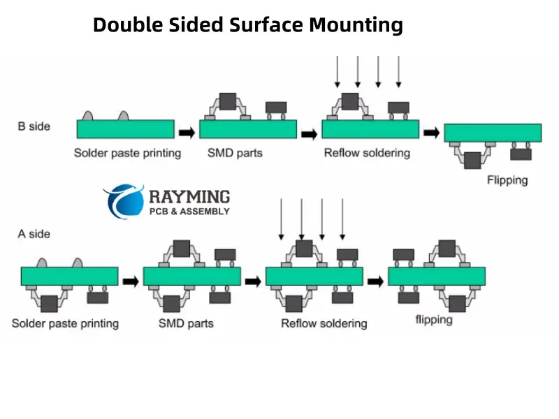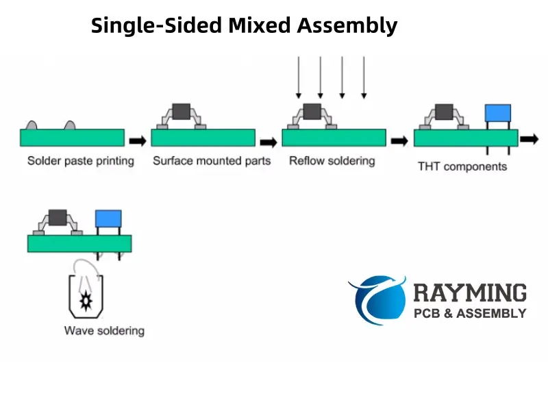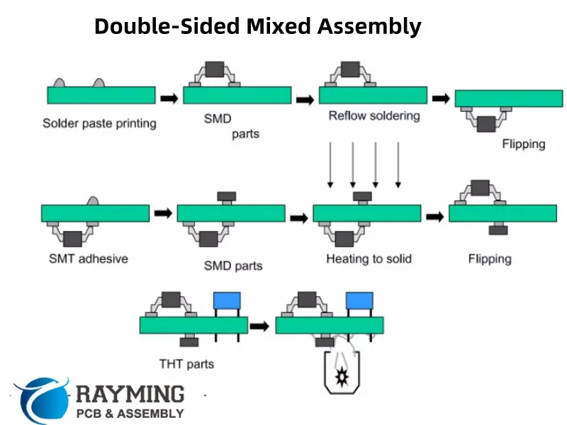

Surface Mount Technology (SMT) is a method of producing electronic circuits where the components are mounted directly onto the surface of the PCB. This process involves several sub-steps:
a. Solder Paste Stenciling

- A stencil is aligned with the PCB.
- Solder paste is applied over the stencil, depositing it onto the board’s solder pads.
- The stencil is removed, leaving precise amounts of solder paste on the pads.
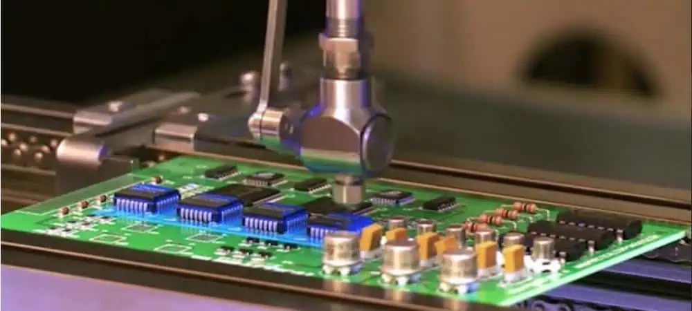
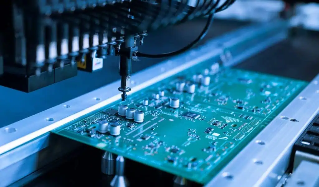
b. SMT Component Placement
- The PCB is loaded into the pick and place machine.
- The machine picks up SMT components from the feeders using a vacuum nozzle.
- Components are precisely placed onto their designated positions on the PCB.
c. Pre-Reflow Automated Optical Inspection (AOI)
- An AOI machine scans the board to check for correct component placement and orientation.
- Any issues detected at this stage can be corrected before the soldering process.
d. Reflow Soldering
- The PCB is passed through a reflow oven with carefully controlled temperature zones.
- The solder paste melts and then cools, forming solid solder joints between the components and the PCB.
e. Post-Reflow Automated Optical Inspection (AOI)
- Another AOI is performed to check the quality of the solder joints and to ensure no components shifted during the reflow process.
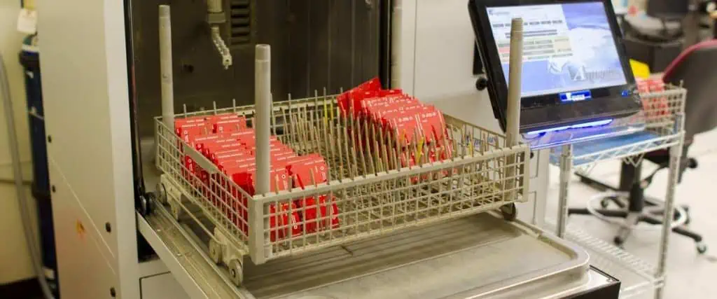
f. X-ray Inspection
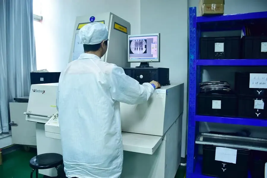
- For complex components like Ball Grid Arrays (BGAs), X-ray inspection is used to check solder joints that aren’t visible from the surface.
g. Wave Soldering
- While primarily used for through-hole components, wave soldering can also be used for SMT components on the bottom side of the board.
- The PCB passes over a wave of molten solder, which adheres to exposed metal areas.
h. Flying Probe Testing (FPT)
- This is an automated electrical test that checks for shorts, opens, and component values.
- It’s particularly useful for low-volume or prototype boards where creating a dedicated test fixture isn’t cost-effective.